Page 5 of 8
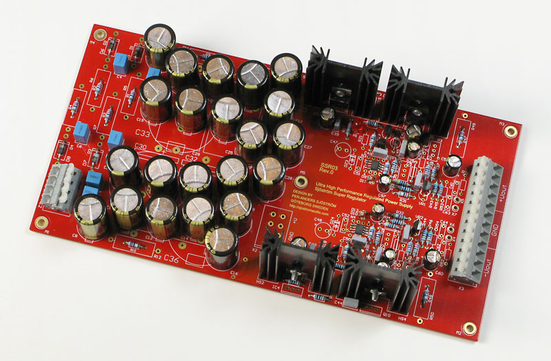
The pcb layout
Click on the picture to get a larger view.
Please download the pdf of the pcb layout for more info.
The pcb is made of 70 um (2 oz.) copper and has two layers. There are groundplanes on both sides and also a special groundplane for the signal ground.
In several places there are room for alternative parts such as regulators and transistors for external heatsinks, DIL08 opamp (N2) and voltage references VR1. Thin outline is for LM329 and bold outline LM431 and other pin compatible parts.
My design SSR01 (similar to this) is in the top of super regulators in the market and one of the best in "jackinnj"'s test in Linear Audio's big regulator test. It's worth noticing that not every regulator had the super regulator topology.

