Build directions
Before you build, take a look at possible component selections and trimming. It doesn't harm to skip this but maybe it feels better in knowing to have a more symmetrical amp than you would have otherwise.
Have you noticed my method of naming the components? The reason why I did this is to limit the length och the parts name. A few components have number above one hundred. It's more difficult to get a clear marking on the pcb if the parts name is too long.
Left channel, right channel
R1 = E1 (resistors)
C1 = G1 (capacitors)
T1 = V1 (transistors)
Q1 = N1 (SMD transistors)
Y1 = U1 (SMD matched transistors)
Above is valid for all components except for (my mistake when I made the pcb):
R27 = E29
R29 = E31
R31 = E27
The amp can be build in two different ways: The big bang method or the cautious method. It's nothing wrong with the big bang method if you are experienced and/or skilled.
The big bang method
Solder in everything and then apply voltage. If you are thorough, the amp works.
If you want to trim anything read this first.
Recommended solder order (just for practical reasons). Start with low components and then take parts with bigger height. If you wait with the transistors you will have rather high caps as distances. This will make it much easier to solder in the transistors nice and straight.
- Transistors (SMD)
- Resistors
- Zeners
- Capacitors, plastic
- Capacitors, electrolytic
- Transistors (hole mounted)
- Connectors
- Opamps, but wait until you have made the first test.
Error reports
Mixed up naming left, right channel but the schematic is correct.
R27 = E29
R29 = E31
R31 = E27
Esthetic error in the pcb
G56 and G57 have changed physical positions. G56, 57, 58 are all parallel connected. If you want it to "look right", let G56 and G57 change positions.
Z11 has the lost the last "1" because the pcb manufacturer removes all print in the pads.
Error in the pcb
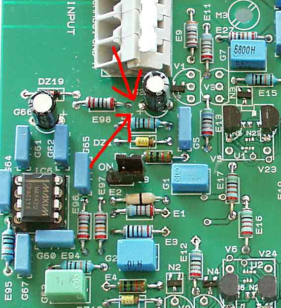
This error is fixed in the second production batch. E98 has a missing trace towards +15 volts. Correct this with a short wire (use the leg of E98!) on the solder side. See pictures below.
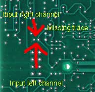
Click on the picture to get a larger view.
The cautious method (recommended for most people)
If you want to trim anything read the section about trimming first.
Solder in all passive parts. Then solder some active parts and then test the function. If it's OK solder in more parts. This method is quite good if you have bought my rather expensive pcb's and want to have a nice looking result.
Recommended solder order
Recommended solder order (just for practical reasons). Start with low components and then take parts with bigger height.
- Resistors
- Zeners, match (if you want to) each pair DZ1 and DZ2, DZ5 and DZ6, DZ11 and DZ12, DZ15 and DZ16. The zeners should have the same value pairwise. Match them with same current as they will have in the circuit. Take 10 kohms in series and 15 or 18 volt.
- Capacitors, plastic
- Capacitors, electrolytic
- Connectors
- Transistors (hole mounted and/or SMD), see text below. Hole mounted transistors should have short legs, 5 mm is max. It's recommended to have a compact design. The transistors are more protected and the RF-rejection is improved (shorter antennas).
- Opamps, but wait until you have made the first test.
Check one channel
Check one channel at the time. Start with the left channel. The building advice is for the left channel but the same goes for the right.
Solder first everything except for transistors. You can also solder all the components which are connected to the transistors in mind but it's no danger to solder all passive components first. Maybe it's easier to get an overview if not all passive components are in place.
Start to check the preamp, then the RIAA-amp, one channel at the time. Note that you can apply voltage to one channel at the time.
- The transistors for the input stage. Start with T1-T26. Place a jumper at J1. The input will be more or less shorted. Apply voltage and measure the DC-voltages but bare in mind that the stage has a certain unbalance because it has no feedback.
- After that take T27-T36. Place a jumper at J1. The input will be more or less shorted. Apply voltage again and measure the DC-voltages. Now the amp has feedback but it should still have a minor unbalance, DC-voltage at the output. Up to 1 V at the output (TP1) can be expected.
- Check the range of the DC-servo. Apply 15V at pin 6 of IC1, and of course, no opamp in place. You should get a negative voltage at the output. Apply -15V at pin 6 of IC1. You should get a positive voltage at the output. If you don't get negative and positive output voltage you must lower the value R27, R28, R29 and R30. The DC-servo won't work otherwise. You must have symmetrical values of these resistors. R27 and R28 can have one value and R29 and R30 an other. Change the value in small steps. I think 68 kohms will cover all situations but it's less interfering with high values.
- Insert the IC1 opamp. Apply voltage. The output offset should be the same value as the opamp itself. < 0.5 mV is good but you set the limit for what it's good. I recommend that you don't use IC sockets and if you still want use high quality with "tulip" contact. I have used sockets only for development. Don't use them!
- Insert the IC5, chopper stabilized opamp for the input bias current servo amp. You can also use a slow low noise precision opamp but remember to remove the zeroing caps, C61, C62. If you use a normal opamp you don't need the zeners either, DZ9, DZ10.
- Check the servo. Apply J1. Apply voltage and have a voltmeter at the output, TP1. Remove the jumper and observe the output transient. After a while the output should be zero. This will take some time. If you test with a MC pickup (or a low resistance it will take minutes. The servo is necessary with super low noise transistors both with MM and MC pickup and with MM pickup with BCxxx transistors. With BCxxx and MC it's not a problem with base currents.
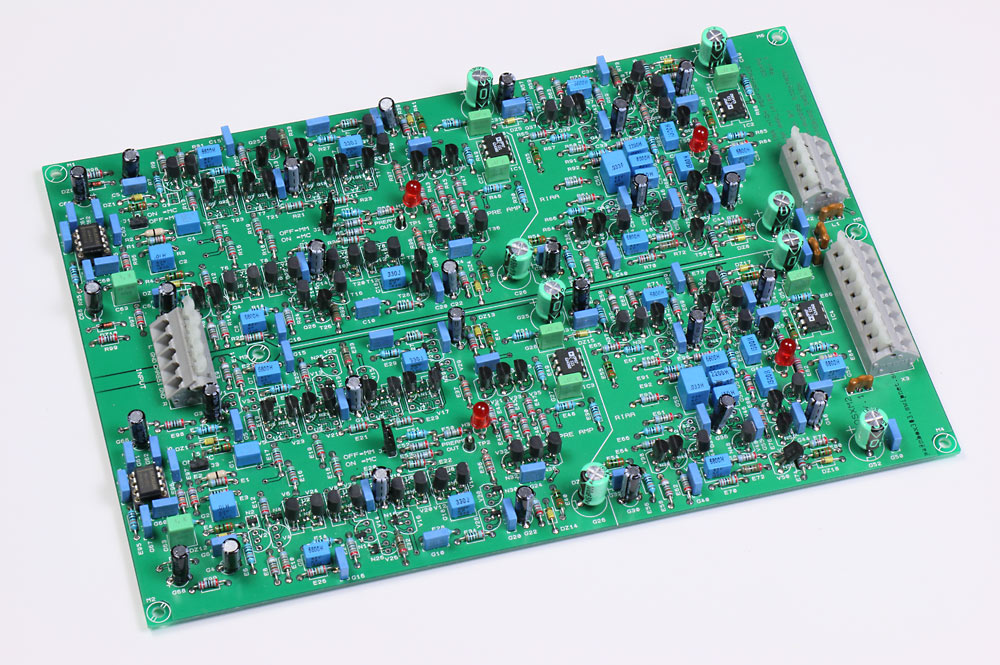
The whole pcb
Click on the picture to get a larger view.
The complete phono amp with all components soldered in. The right channel (lower half of the pcb) has some SMD transistors. This is only for the picture taking.
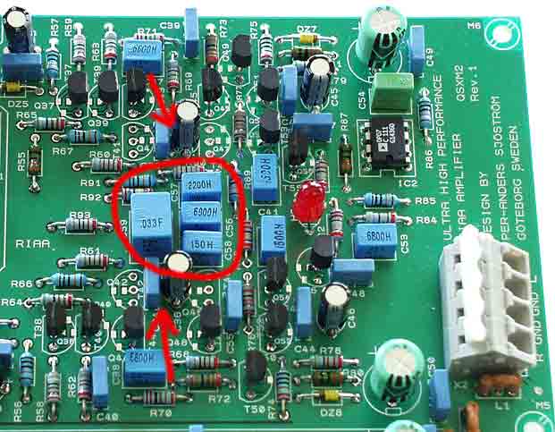
The RIAA amp
Click on the picture to get a larger view.
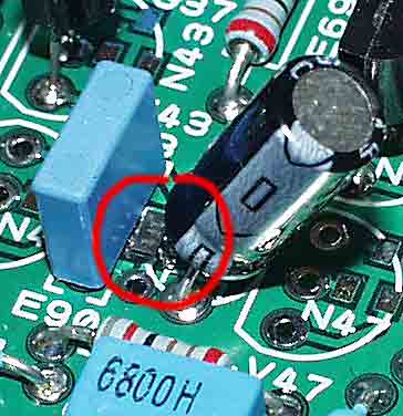
Detail of the RIAA amp. The marked capacitors are the RIAA correction network. It's important that those caps have low tolerance, or measured.
SOT-23, surface mounted transistor
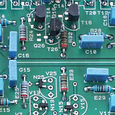
Click on the picture to get a larger view.
Here is a detail of the SMD transistors. Every transistor can be SMD type if you want or can't get good hole mounted types.
SOT-23 and TO-92, surface mounted and hole mounted transistors
Click on the picture to get a larger view.
Here is an another detail of the SMD transistors.
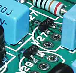
SOT-363 BC847BS, BC857BS, surface mounted matched transistor pair
Click on the picture to get a larger view.
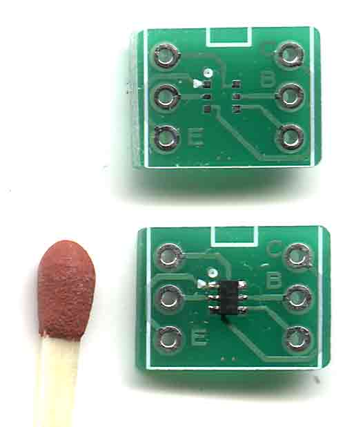
Here is an another detail of the SMD matched transistors pairs with are in the input stages. They are not easy to solder because they are so tiny. The are quite good though if you compare the price. Beware of that this type has no noise parameters. They can be noisier than other types which has specified noise figures. If you plan to use MM pickup only noise figure isn't so important (compared to MC pickup). With 8 pairs the noise will always be lower than needed in MM mode.
Click on the picture to get a larger view.
This picture shows how small BC847BS and BC857BS really are.

