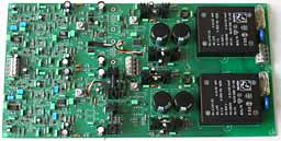
QRV-01 - The extreme headphone amplifier
Click on the picture to get a larger view.
I designed this amplifier 1986 and I felt like publishing it now. The excellent MOSFETs from Supertex Inc are hard to get these days (not impossible) so therefore the amp needed to be redesigned a little bit.
The performance is outrageous in headphone amp terms. See the technical data!
Why a discrete design when an opamp is cheaper and more or less equally good?
- The feeling of a discrete design.
- Fun to design and calculate and tailoring the performance.
- Cool to do something crazy.
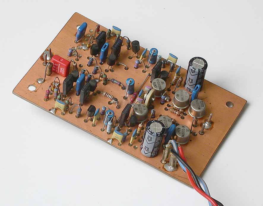
Click on the picture to get a larger view. This is the very original of this headphone amp.
The original pcb was hand taped but now I have put it into the computer and made a CAD pcb. My design goal was not to make a simple amp but a masterpiece with cheap components and a well tested topology.
The amp works in class A as much it's possible. You can listen at all sound levels in pure class A. Despite the fact that there are many components, the amp is very easy to build. I have removed the influence of variation of the components. The only thing that differs is the noise. Some BC5XX transistors have considerably lower noise than others. Check out transistors from ON (Motorola).
If the noise performance isn't good enough, you can use MAT02/03 or JFET's. The noise can then be lowered with 10-20 dB.
Interesting features
In order to get an extremely linear and extremely low distortion design I have taken a couple of measures:
- Symmetrical design
- No capacitors in the signal paths
- Cascodes in the input stage and in the high gain stage
- Buffered cascodes with emitter followers
- Possibility to use ultra low noise transistors
- Possibility to use SMD transistors in SOT23
- High speed output stage with either small DIL mosfets, TO220 or TO126 parts
- Advanced input bias servo
- Totally DC-coupled together with DC-servos and input bias current servo
- Many decoupling capacitors and EMI-filters
- Professional quality printed circuit board with groundplane
- The pcb has lot's of possibilities when it comes to tweaking. You could use JFET's as input transistors for instance.
- A complete dual mono power supply including transformers
The Schematics
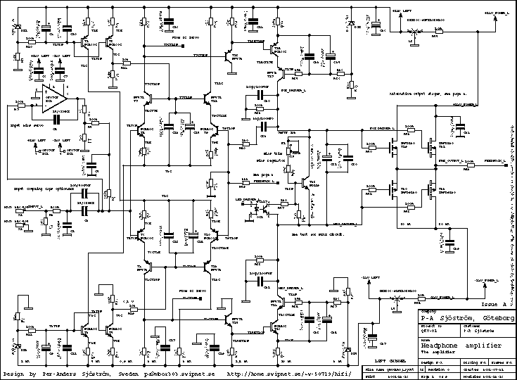
The schematics, page 1 and 6.
Click on the picture to get a larger view. The picture shows the schematics of the amp. Of course you can't use it for anything except for an overview. Please download the pdf-file instead if you want to see the details.
Page 1 and 6 are the main pages. Here are the whole amp except for the optional output stage and the power supply.
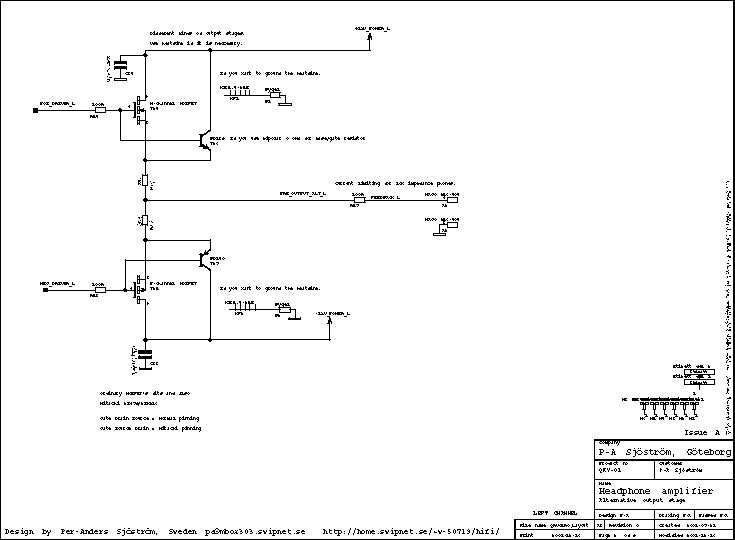
The schematics, page 2 and 7.
Click on the picture to get a larger view. The picture shows the schematics of the amp. Of course you can't use it for anything except for an overview. Please download the pdf-file instead if you want to see the details.
The pcb is equipt with options for a general output stage. You can use MOSFET's, JFET's (if you can find any?) and ordinary bipolars. I have covered three different pinnings so every TO126 or T0220 part will fit as long as the electrical parameters are sufficient.
The schematics, page 3 and 8.
Click on the picture to get a larger view. The picture shows the schematics of the amp. Of course you can't use it for anything except for an overview. Please download the pdf-file instead if you want to see the details.
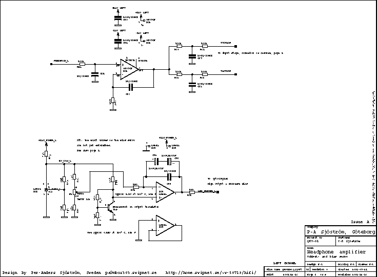
The DC-servo and the temperature regulation circuit.
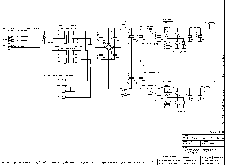
The schematics, page 4 and 9.
Click on the picture to get a larger view. The picture shows the schematics of the amp. Of course you can't use it for anything except for an overview. Please download the pdf-file instead if you want to see the details.
The stabilized power supply. Note that there is an option for using a low profile transformer or for a "normal" one.
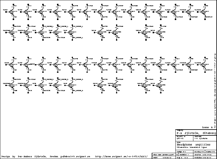
The schematics, page 5
Click on the picture to get a larger view. The picture shows the schematics of the amp. Of course you can't use it for anything except for an overview. Please download the pdf-file instead if you want to see the details.
SMD alternatives for all transistors.
Circuit description
The amp (see above and pdf-files) has very low noise (if you equipt the amp with low noise transistors) and an extremely flat frequency response, up in the megahertz-region. The input impedance is determined by the input bias servo. With the chosen resistor values the input impedance is 200 kohms.
In order to get an extremely linear and extremely low distortion design I have taken a couple of measures:
- Symmetrical design
- No capacitors in the signal paths
- Cascodes in the input stage and in the high gain stage
- Buffered cascodes with emitter followers
- Possibility to use ultra low noise transistors
- High speed output stage of four different kinds, small MOSFET's, larger ones, and bipolar transistors of virtually any kind as long as they are of TO220 or TO126 type.
- Input bias servo
- Totally DC-coupled together with DC-servos and input bias current servo
- Many decoupling capacitors and EMI-filters
- Built-in power supply including transformers
- Professional quality printed circuit board with groundplane
Symmetrical design
The whole amp is completely symmetrical (not entirely because of the fact that NPN and PNP never will be their exact opposites) with help from PNP- and NPN-transistors. The benefit of a symmetrical design is lower distortion and I like symmetrical designs, just by the looks.
No capacitors in the signal paths
Two DC-servos eliminates the input offsets, which always are present. No capacitors are the signal path. Therefore the output offset voltage is about 10 times higher than in a normal AC-coupled amp. The residual offset comes from the DC-servo and the opamp. The output offset voltage is the DC-voltage at the output when you have no signal applied to the input. It comes from deficiencies in the input stage times the total DC-gain. In my case it is some millivolts times the closed-loop gain. The offset comes from differences in the input transistors characteristics, temperature, DC-gain etc. It's impossible to make two identical transistors. There is always a difference between two transistors. You can minimize the defect by having two or more transistors on the same chip. Examples of very good matched monolithic transistor pairs are SSM-2210 (not available anymore) and same type in metal can MAT02 (NPN) and the PNP-types SSM-2220/MAT03. The difference is only DIL08 plastic package and TO-78, metal can....and the price I must add!.....1,5 vs 10 dollars! I have tested with good results the ultra tiny BC847/BC857BS but these transistors are not suitable for newbeginners because thet are so tiny. See the picture!
Is there anyone who knows if there are alternatives to MAT02/03?
Input bias servo
To reduce the output offset voltage further the amp has also a circuit which injects DC-current to the input. The input currents are not negligible if ultra low noise transistors are used. If you are going to use normal BCxxx transistors there is no need really for this servo but I doesn't hurt to have them.
Cascodes
The cascode stage is a very useful combination of two transistors. The benefits are two, lower distortion and dramatically extended frequency response. T15 and T17 is one of the cascodes. The gain is 20000(!) and the bandwidth 20 kHz. Maybe it's not that interesting to know why the stage gets faster, but it's true. But why does the distortion decrease?
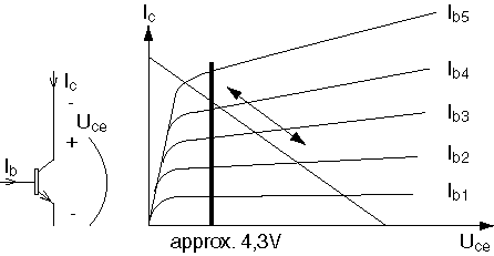
The bipolar transistor is a current driven device. You are only interested in input (base) current and output (collector) current. The picture above shows that the current gain is dependent of the applied voltage on the collector. If i.e. Hfe is 300 at 1 mA and 25V, it gets 350 at 35 volts. The current gain isn't a constant parameter. It changes also if you change the base current. 10 uA base current generates 1 mA, 20 uA, 2,2 mA, 30 3,6 mA. The fact that the current gain isn't constant generates harmonic distortion. But the greatest "defect" is the sensitivity for varying collector voltages.
If you take out the output signal at the collector with a help from a collector resistor, you'll get a signal that moves along the load line, see above. The graphical way of showing it is that the lines for Ib1, Ib2 etc. gets more separated at higher collector voltages, at the right. This is a sign that the current gain is higher than at the left (low collector voltages). Parallel, but maybe inclining, lines is a sign of constant current gain.
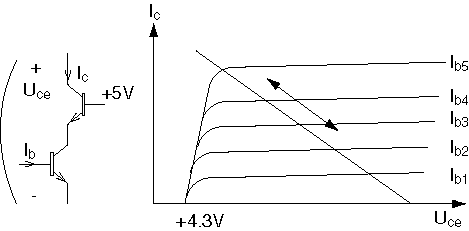
If you try to keep the collector voltage constant and in some way try to use the collector current you get interesting results. The "magical" load is the input of a base grounded stage. The base is at a constant potential with respect to signal ground. The input impedance of a such stage is very low, 25 ohms at 1 mA, 2,5 ohms at 10 mA. The base grounded stage isolates the first transistor from collector voltages variations.
The results of this are:
- Elimination of the Miller effect and therefore increases (extends) the frequency response dramatically
- Reduction of distortion
- Creates a super transistor with high gain, high voltage and high speed and also high power in some circumstances.
Advantage to use cascodes in an input stage:
- Faster input stage and therefore easier to feedback and to get a stable combination. The input stage should be as fast as possible.
- Possibility top use low voltage and low noise transistors and high supply voltage, especially important in power amplifiers.
Advantage to use cascodes in a high gain stage:
- Possibility top use low voltage and fast transistors together with high voltage ones and achieve high gain at high voltage swings.
- Low distortion
- Faster stage (sometimes an advantage)
Explanations of the specific design
Please download all the schematic pages and print them out. It's much easier to understand what I'm talking about if you look at the circuits at the same time. I will only talk about the left channel and the upper half. The design is symmetrical and the two channels are identical.
The input filter
The input filter is for "just in case" but still it's very wise to have it. If you choose to use the input bias servo the input impedance will be 100 kohms (R3) and if you choose not it's several megaohms (you can ignore it).
R1 is a pulldown resistor if not coupling caps (C2, C3) or input bias servo are used.
R2 together with C1 is an EMI-filter. In order to achieve the lowest noise possible (not very important in this application) R2 should be 0 ohm if you don't have any RF interference. I recommend that you always has this filter.
The differential (input) stage
Current source for the stage is DZ2 sets a 6.8 V voltage, fed through a LP-filter (R11, C9, C11) with reduces noise from zener and power supply and makes the amp start up nice when the power is switched on. The voltage drop across R11 is approx. 0.7 V. This makes a voltage across R13 of 5.56V. The current is therefore 3,7 mA divided into two parts feeding the differential transistors (T5, T9) which can be separate components or monolithic and matched pairs.
T7 and T11 forms a cascode together with the lower transistor pairs, T5 and T9. This type of stage extends the frequency response by a factor of at least 10. The distortion is also reduced. T3 creates a constant current and a constant voltage across R16 related to ground. The voltage is approx. 5.5 V. T7 and T11 are biased via R18 and smoothed by C11 and C14.
In order to get higher speed of the input stage, the emitters of T5 and T9 have resistors (degenerated emitters). This reduces also the gain and like a bonus also the distortion.
The gain is (due to the emitter resistors) R22/(R20*2) = 6, 15.5 dB.
The noise performance is the best at 100-300 µA with BC550/560 transistors. 1 mA or more is better for speed (easier to avoid oscillations). If you use MAT02/03 the optimum current is approx. 1-5 mA. If you choose to use MAT02/03 I recommend 1 mA through each transistor. Don't forget to recalculate the associated resistors.
The emitter follower after input stage and cascode
The emitter follower T13 decreases the effect of the load from the high gain stage T15 and T17. The result is mainly extended frequency response of the first stage. The second result is lower distortion. The main advantage of the emitter follower is increased phase margin and therefore better stability when the whole amp is feedbacked. The odds not to have oscillations increases.
The frequency response of the emitter follower is very high (>> 10 MHz) and also a little bit tricky to measure it.
The high gain stage
The important high gain stage is formed by T15 and T17. A minor local feedback is created by R30. The total gain is quite extreme, approx. 20000 times! The gain is lowered further with R32. The result is gain determined by R30/R32 = 1000 (60 dB). C20 creates a dominant pole in order to get a stable amplifier when feedbacked. The gain is very easy to adjust, just change the relationship between the mentioned resistance's. It's possible the lower the capacitance's in order to get a faster stage and lower the distortion. An easy way to test how small the capacitance can be, apply square wave and trim for a perfect step response. The value of C20 is a compromise in order to have speed but no oscillations. Chosen value is safe in order to avoid unstability, no gambling.
The fast output stage
I have chosen four different kinds of power transistors.
- DIL-04 small cute MOSFET's
- GDS, Ordinary pinned power MOSFET's
- GSD, "Hitachi" pinned power MOSFET's like 2SJ79, 2SK216
- ECB, TO126 types like BD139/BD140
The small IRFD120/9120 are my substitutes for the orginal Supertex MOSFET's but I figured that much that it would be smart to design a 100 % universal output stage. These IRFD120/9120 are kind of odd with it's package DIL-04. You will get good performance of every kind of output stage. It's more like a matter of taste.
The bias circuit
The bias circit is made of a common Vbe multiplier and the transistor (BC550 like) is either glued to one of the IRFD120 fet's or mounted on heatsink but then you may use BD139 as sensing element.. If you use MOSFET's is't an advantage to use a MOSFET as sensing element because temperature coefficient will be more alike. If you use a bipolar transistor with MOSFET's you will get an amp which has high start current. No harm in that but it's maybe nicer to have constant current.
Unfortunately the class A temperature regulation circuit needs more development. Forget it for now! The main problem with the regulator is current limiting. You must sense the current somehow.
DC-servo
It's virtual impossible to get good DC-performance without some kind of servo (based on good opamps). The servo has no problem to be connected conventionally to the junction of the inverting input (base of T9, T10) but I prefer the chosen technique.
I have chosen to inject current inside the amp instead. Through R60, R61 a small current is either injected or drained. C37 makes sure that no audio signal goes into the servo and also that the servo not introduces any noise. The opamp IC2 should be a decent type with good DC-performance, slow and with low noise. The speed of the opamp should be not more than 1 V/µs. The opamp works as a non-inverting integrator. You should always have symmetrical component values in order to get a true integrator and also to get low offset caused by input offset currents of the opamp.
Input bias servo
Because the input stage has noticeable input current, an offset voltage is always present. If ultra low noise transistors are used, this servo is very important because of the high base current from the negative half. The PNP types of this transistor type has rather low current gain and the NPN-type rather high. This causes an unbalance in base currents. IC1 works a normal inverting integrator which strives to keep the output of the opamp at zero volts. The servo speed is very dependent of the signal source impedance. Very low source impedance creates very long time constants. If the R2 of the input filter is decreased the servo gets even slower.
Feedback
The total open-loop gain is 6000, 75.5 dB and the closed-loop, 11,(= 20.8 dB). The closed-loop gain is set by (R49/R51) + 1, a little bit high maybe but it can be decreased without any problems. 1-10 is normal gain values. My Sennheiser HD545 needs 2-4 times in gain for 1 V signal sources in order to play real loud.
SMD types, alternative transistors
Long time ago (in 1986) when I first designed this amp it was very easy to get good hole mounted types of transistors but now it can be quite hard to get good transistors with high gain. It's rather easy though to get good surface mounted types. Therefore I have made room for SMD types in every transistor position. I have also included the possibility to use cheap transistor pairs (very small devices) and for matched ultra low noise matched pairs. SMD transistors aren't so hard to solder by hand but BC847BS/BC857BS are not suitable for newbeginners, only if you are VERY handy with the soldering iron.
Rescently when I was soldering the prototype I discovered that the video transistors BF471/BF472 are out of production since a couple of years! I can't find any TO126 type with similar characteristics (extremely low Cbc). You can use ordinary TO92 types but I have made any room for these. You can mount them in the TO126 holes but it doesn't look so nice. You could also you SMD transistors. They will fit.
Power supply
... more to be said......Note that there is an option for using a low profile transformer or for a "normal" one.
Component choices
I have nothing against "audiophilic" components but this design requires normal standard good performing industrial parts as a good start and will work correctly if the recommend parts are used. Feel free to change the parts you like but you must have control over the important electrical parameters of each part. I think that some of the "audiophilic" parts are just plain froud. They have absolutely no documented "audiophilic" features what so ever. Same parts are only known but rumours over the internet and magazines. In many cases no double blind tests have taken place.
The pcb layout
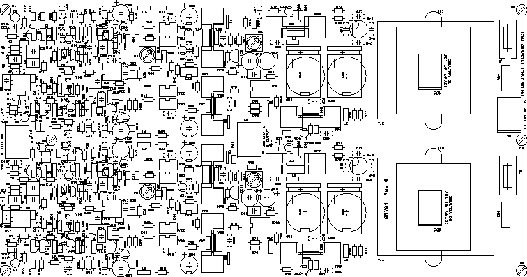
The component print
The picture shows the component print of the PCB. Of course you can't use it for anything except for an overview. Please download the pdf-file instead if you want to see the details.
The printed circuit board is made for two channels, contains everything, transformer, power supply and the amp itself except for connectors. I have chosen not to have pcb mounted headphone and phono connectors because it's hard to fit in a case. My goal here is the use a 1 HE high case. The pcb have groundplane on the upper side (not shown in pictures) which is essential in order to get good results.
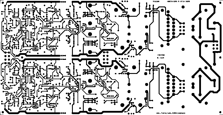
The solder side
The picture shows the solder side of the PCB. Of course you can't use it for anything except for an overview. Please download the pdf-file instead if you want to see the details.
Almost everyone of the traces are on the solder side. The groundplane is very covering, only a few traces on the component side, see below.
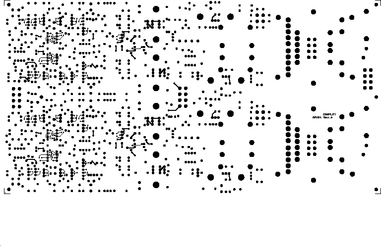
The component side
The picture shows the component side of the PCB. Of course you can't use it for anything except for an overview. Please download the pdf-file instead if you want to see the details.
Almost everyone of the traces are on the solder side as you can see. The groundplane is very covering, only a few traces on this side.
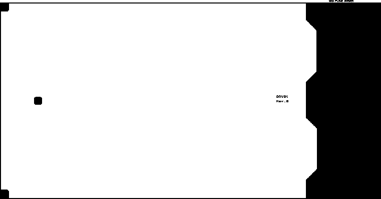
The groundplane mask
The picture shows the groundplane mask of the PCB. Of course you can't use it for anything except for an overview. Please download the pdf-file instead if you want to see the details.
The black area is without groundplane, mainly under the transformers.
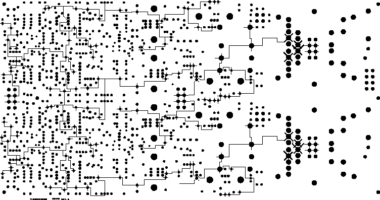
The hot relief pads
The picture shows the pads which are connected to groundplane of the PCB. Of course you can't use it for anything except for an overview. Please download the pdf-file instead if you want to see the details.
Each "cross" at the pads is a ground connection. This file is used together with the component side in a sandwich. I use this technique because my cad program has a very slow groundplane generation.
Build directions
Click on the picture to get a larger view.
Before you build, take a look at possible component selections and trimming, also take a look at the error report. It doesn't harm to skip this but maybe it feels better in knowing to have a more symmetrical amp than you would have otherwise.
Have you noticed my method of naming the components? The reason why I did this is to limit the length och the parts name. A few components have number above one hundred. It's more difficult to get a clear marking on the pcb if the parts name is too long.
Left channel, right channel
R1 = E1 (resistors)
C1 = G1 (capacitors)
T1 = V1 (transistors)
Q1 = N1 (SMD transistors)
Y1 = U1 (SMD matched transistors)
MT = MT (Matched transistor pairs, the same in both channels)
The amp can be build in two different ways: The big bang method or the cautious method. It's nothing wrong with the big bang method if you are experienced and/or skilled.
The big bang method
Solder in everything and then apply voltage. If you are thorough, the amp works.
Recommended solder order (just for practical reasons). Start with low components and then take parts with bigger height. If you wait with the transistors you will have rather high caps as distances. This will make it much easier to solder in the transistors nice and straight.
- Transistors (SMD)
- Resistors
- Zeners
- Capacitors, plastic
- Capacitors, electrolytic
- Transistors (hole mounted)
- Transistors with heatsinks
- Regulators with heatsinks.
- Connectors
- Transformers
- Opamps, but wait until you have made the first test.
Error reports
Mixed up naming in the pcb but the schematic is correct.
E7 and E17 has switched positions at the pcb. The text "E7" and "E17" have been switched to be more exact. When I did the pcb I moved around the designators so they would be readable but in this case I messed it up.
Esthetic error in the pcb
The transistors Y9, N9 are slightly under E24, R24. Solder the transistors first.
The cautious method (recommended for most people)
Solder in all passive parts. Then solder some active parts and then test the function. If it's OK solder in more parts. This method is quite good if you have bought my rather expensive pcb's and want to have a nice looking result.
Recommended solder order
Recommended solder order (just for practical reasons). Start with low components and then take parts with bigger height.
- Resistors
- Zeners, match (if you want to) each pair DZ1 and DZ2, DZ3 and DZ4, DZ5 and DZ6, DZ7 and DZ8. The zeners should have the same value pairwise. Match them with same current as they will have in the circuit. Take 10 kohms in series and 15 or 18 volt.
- Capacitors, plastic
- Capacitors, electrolytic
- Connectors
- Transistors (hole mounted and/or SMD), see text below. Hole mounted transistors should have short legs, 5 mm is max. It's recommended to have a compact design. The transistors are more protected and the RF-rejection is improved (shorter antennas)
- Regulators with heatsinks.
- If you don't use DIL04 MOSFET's, mount heatsinks and power transistors.
- Transformers
- Opamps, but wait until you have made the first test.
Check one channel
Check one channel at the time. Start with the left channel. The building advice is for the left channel but the same goes for the right.
Solder first everything except for transistors and opamps. Wait also with the heatsinks for the power transistors but only if you not choose DIL04 MOSFET's. You can also solder all the components which are connected to the transistors in mind but it's no danger to solder all passive components first. Maybe it's easier to get an overview if not all passive components are in place.
Start to check one channel at the time. Note that you can apply voltage to one channel at the time.
VARNING THIS TEXT ABOUT CHECKING ISN'T READY YET!
- The transistors for the input stage. Start with T1-T26. Place a jumper at J1. The input will be more or less shorted. Apply voltage and measure the DC-voltages but bare in mind that the stage has a certain unbalance because it has no feedback.
- After that take T27-T36. Place a jumper at J1. The input will be more or less shorted. Apply voltage again and measure the DC-voltages. Now the amp has feedback but it should still have a minor unbalance, DC-voltage at the output. Up to 1 V at the output (TP1) can be expected.
- Check the range of the DC-servo. Apply 15V at pin 6 of IC1, and of course, no opamp in place. You should get a negative voltage at the output. Apply -15V at pin 6 of IC1. You should get a positive voltage at the output. If you don't get negative and positive output voltage you must lower the value R27, R28, R29 and R30. The DC-servo won't work otherwise. You must have symmetrical values of these resistors. R27 and R28 can have one value and R29 and R30 an other. Change the value in small steps. I think 68 kohms will cover all situations but it's less interfering with high values.
- Insert the IC1 opamp. Apply voltage. The output offset should be the same value as the opamp itself. < 0.5 mV is good but you set the limit for what it's good. I recommend that you don't use IC sockets and if you still want use high quality with "tulip" contact. I have used sockets only for development. Don't use them!
- Insert the IC5, chopper stabilized opamp for the input bias current servo amp. You can also use a slow low noise precision opamp but remember to remove the zeroing caps, C61, C62. If you use a normal opamp you don't need the zeners either, DZ9, DZ10.
- Check the servo. Apply J1. Apply voltage and have a voltmeter at the output, TP1. Remove the jumper and observe the output transient. After a while the output should be zero. This will take some time. If you test with a MC pickup (or a low resistance it will take minutes. The servo is necessary with super low noise transistors both with MM and MC pickup and with MM pickup with BCxxx transistors. With BCxxx and MC it's not a problem with base currents.
VARNING THIS TEXT ABOUT CHECKING ISN'T READY YET!
The whole pcb
Click on the picture to get a larger view.
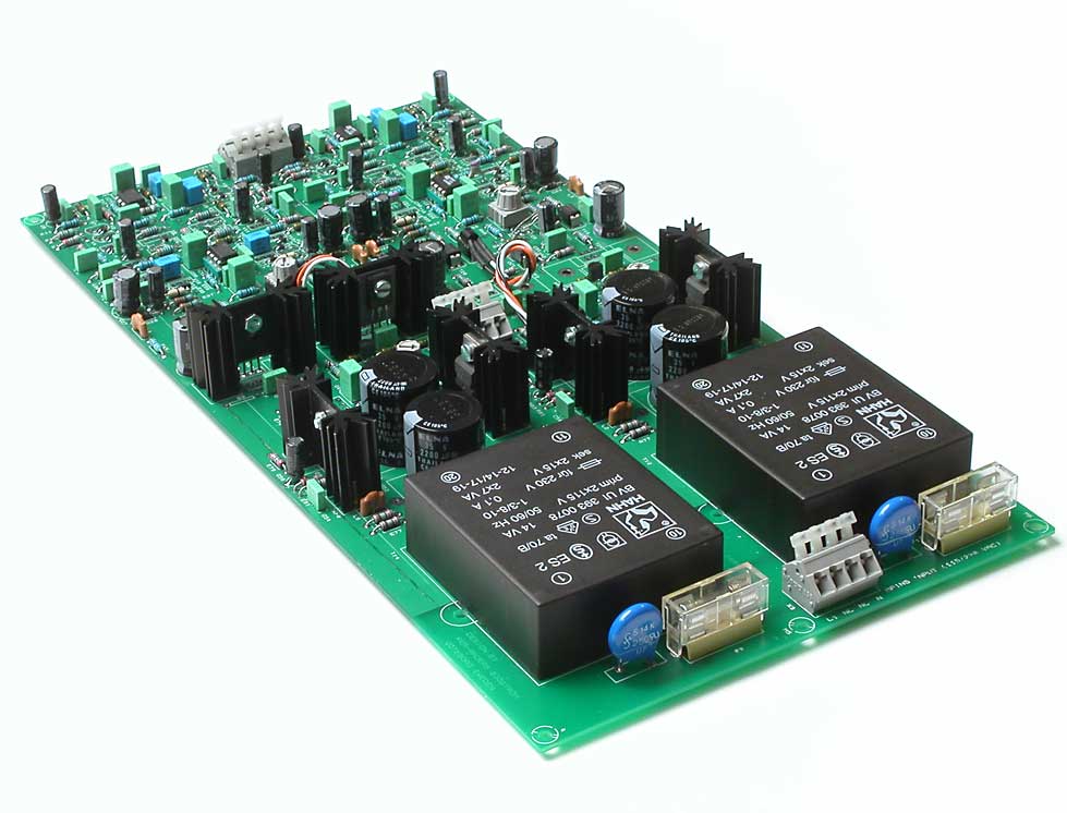
The complete headphone amp with all components soldered in. The pcb has different looks left, right channel. The left channel has DIL04 MOSFET's and the right has bipolar power transistors on heatsinks. This is only for the picture taking.
The temperature sensing transistor
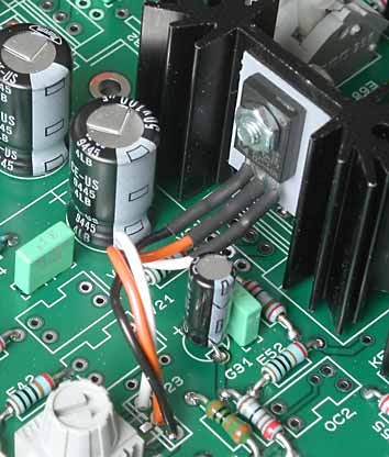
The picture shows how you should mount the temperature sensing transistor. Use isolation (I used silicone rubber) and isolate also the transistor pins with shrink tube.
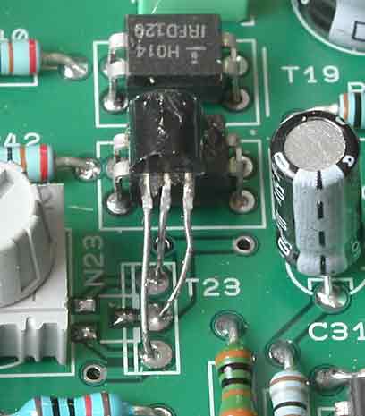
DIL04 mosfets with a temperature sensing transistor.
This picture shows how you should mount the temperature sensing transistor for the DIL04 MOSFET's. The transistor is glued with "contact glue", kontaktlim in swedish. I think almost any glue will do but it must withstand some heat. I used a bipolar transistor but you can also use a small signal MOSFET like for instance BS170 or similar. The advantage of having a MOSFET is that the idle current will be more constant when the amp is getting hotter. The advantage of using a bipolar is that the amp gets very temperature stable. This is not advisable in a normal power amp but in this case is quite OK because the amp works very much in class A regardless of load and signal level.
The tiny BC847BS and BC857BS in package SOT-363, the surface mounted matched transistor pair
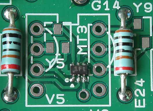
The tiny BC847BS and BC857BS in package SOT-363, the surface mounted matched transistor pair
This transistor is so small and it requires skills in soldring. This is not for a newbeginner. These transistors are really good compared to the price. You will get very small problems with temperature gradients but they are reduced heavily by the DC servos. It's not a big problem really. Beware of that this type has no noise parameters. They can be noisier than other types which has specified noise figures. In this particular design, the noise figure is not very important.
How small are the BC847BS and BC857BS? Click here.
If you want to use super macthed, ultra low noise transistors, you can use MAT02 and MAT03 but this is only interesting if you have higher gain. There is no need for it in a headphone amp. If you do use these transistors you must recalulate some resistor values in order to take advantage of the low noise properties.
Compensation capacitors
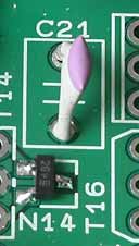
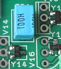
This part C20, C21, G20, G21, is rather sensitive when it comes to performance. You can either use a good NP0 ceramic capacitor or a polypropulene, the blue one. I'll guess other types will do, even silver mica!
Alternative smoothing capacitors
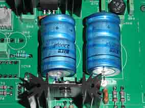
I have made an option for the smoothing caps. You can either choose axial caps like those in the picture or you can use radial ones. This is only a matter of taste and/or supply. Maybe it can be easier somewhere in the world to get axial capacitors.
Listening experience
How important is really the headphone output? It is important! Most headphone outputs are either attenuated loudspeaker outputs (tends to be noisy!) or poor opamps. They are not very often serious because the headphone output is a low priority feature.
As always you can use NE5534, LT1115, OPA627, AD797, AD8610 (many good opamps to choose from) plus a buffer stage, etc. and achieve incredible good results. If you use NE5534 the price/performance ratio is unbeatable.
My goal here was not a cheap nor a simple headphone amp. It has been really fun to design every part in the amp. The whole design is good but totally insane. I guess this amp would be impossible to sell if it was a commercial product, but as DIY everything is possible.
How does it sound really? People out there on the internet just dismiss this amp right away of one simple reason: Too many parts. It's a theory out there that every part has influence on the sound and many parts therefore degrade the sound more. I say that they are not completely right. Noone of those persons has listened to my monster. In fact noone who has listened to this amp has disliked it, on the contrary!
With my Yamaha HP-1? (don't remember the exact number) headphones the original amp sounded splendid. With my Sennheiser HD545 reference it sounds really good! I haven't got so many words for how I experience the sound. I have connected my headphones directly to my DAC and then compared the difference between the DAC and DAC plus this amp. The DAC is capable of driving headphones directly. I must say that I can't hear any difference at all. It's totally transparent! Because of the internal speed, the amp sounds splendid even in class B!! Unbelievable! In class A, the sound is just wonderful, very very small difference compared to class B. The amp sounds a lot better than it looks like (according to some).
What about the mosfet output stage compared to ordinary bipolar? The difference is none, very similar, although I simply like mosfet's more. Can't explain why.
The performance is outrageous in headphone amp terms. The technical data speaks for itself.
Technical data
Original data with Supertex MOSFET's. The new design will differ slightly.
| Frequency response: | 0 Hz - 970 kHz, -3 dB, (7,3 MHz -6 dB) |
| Frequency response with input filter | 3,5 Hz - 47 kHz, -3 dB |
| Power bandwidth at 10Vrms, 50 ohms: | 0 Hz - 970 kHz, -3 dB |
| Equivalent input noise: | 630 nV (100 nV with low noise transistors) |
| Signal to noise ratio: | 103 dB (119 dB) |
| Dynamic headroom: | 123 dB (142 dB) |
| Distortion: | < 0,001 % |
| Slew rate: | 125 V/us (286 V/us uncompensated) |
| Step response: | Perfect without overshoot |
| Gain: | 11 (21 dB) |
| Input impedance: | 100 kohms |
| Input impedance: | > 2 M ohms without offset trim |
| Output impedance: | 3 milliohms |
| Damping factor: | 16000 with 50 ohms load |
| Output current: | 7 A peak |
| Supply voltage: | +- 16-20 V |
| Dimensions: | 315,0 (12,4") x 162,6 (6,4") mm |
E7 och E17 förväxlade i kortet. Fixat i CAD ej publicerat
Strömgenerator värden olika mellan positiv och negativ halva, fixat i cad, ej publicerat
R24, E24(?) ovanpå SMD transistor
6.8k -> 10 kohm bias MOSFET 1 kohm BJT
Skriva om nätdelen och val av trafo

