Page 6 of 7
The PCB layout
Click on the picture to get a larger view.
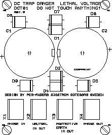
The component print

The picture shows the component print of the PCB. Of course you can't use it for anything except for an overview. Please download the pdf-file instead if you want to see the details.
TThe printed circuit board is made of 95 um thick copper. As you can see at the picture the pcb will be at mains potential and therefore lethal. You must insure that this pcb is well protected against unintentional touching. All parts are dangerous to touch when the mains is on..
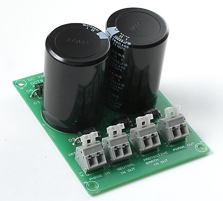
The component side

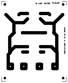
The solder side

The picture shows the component side of the PCB. Of course you can't use it for anything except for an overview. Please download the pdf-file instead if you want to see the details.
Most of the traces are on the solder side.

