DCT-01 The DC trap, DC filter, high-end style
Click on the pictures to get a larger view.
Do you have an amplifier with a (sometimes) buzzing toroid transformer? This DC trap or DC filter removes or at least lowers the buzzing.
Interesting features:
- Room for up to 2 x 10000 uF snap-in high performance caps.
- Two DC blocking voltages.
- Very thick copper traces, virtually impossible to burn off.
The background
Click on the pictures to get a larger view.
Why does the transformer hum
Why does especially the toroid transformer hum, sometimes hard? The iron core is very efficient and the magnetic flux is high, very near magnetic saturation of the core. This gives very little room for "extra" flux which DC can cause. DC on AC mains is simply unsymmetrical waveform of the sinus wave. What happens if you have a hair drier with half speed? This is accomplished with a diode and halfway rectification, causing the positive peak voltage become lower than the negative. This creates a small DC level which some apparatus don't like, especially toroids. An another reason for DC on the mains is switching transients in large networks.
The DC trap makes sure that no DC slips through. The primary winding is AC coupled with help from two big electrolytic capacitors. The inrush current will go through the diodes when the capacitors have been charged over 1 or 3 volts and the normal current will only go through the capacitors.
The schematics
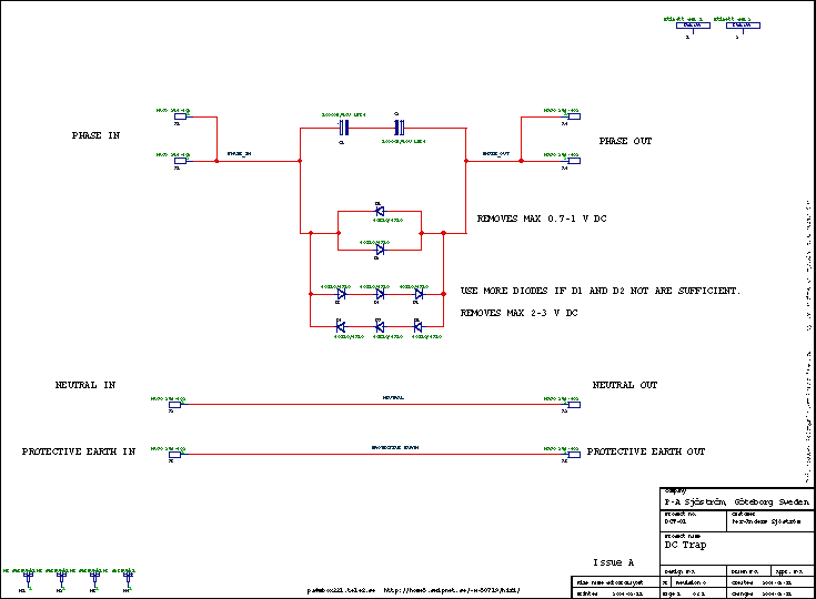
Click on the picture to get a larger view. The picture shows the schematics of the amp. Of course you can't use it for anything except for an overview. Please download the pdf-file instead if you want to see the details.
WARNING - CAUTION
As you can see at the picture the pcb will be at mains potential and therefore lethal. You must insure that this pcb is well protected against unintentional touching. All parts are dangerous to touch when the mains is switched on.
Circuit description
This design is very simple, just a couple of diodes and capacitors. I have made room for two options in terms of DC level. Use only D1 and D2 if this is sufficient. If you have no opportunity or won't risk anything, go for D3-D8 right away. The only disadvantage is a slightly higher cost. If you of some reason want to go from two diodes to six, just cut away D1 and D2. Don't try to desolder. You will only damage the pcb.
X1 and X4 are 2-pole just because they are separated and the connector has two poles. No need for the extra pole really.
I have added room for three wires in and three wires out. Neutral and Protective Earth can be connected also just as a joint between incoming mains cable and the internal wiring.
Build directions
Click on the picture to get a larger view.
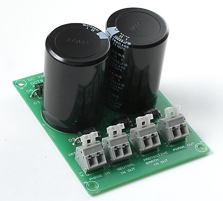
This design is very easy to build, just mount and solder everything. Decide for yourself if you want two or six diodes. The pcb requires much heat due to the thick copper traces. Don't be scared to really "burn" the solder joints. Make sure that the tin is really melting and form nice and shiny looking joints.
Test
Click on the picture to get a larger view.
----- Please notice this first!-----------
WARNING - CAUTION
As you can see at the picture the pcb will be at mains potential and therefore lethal. You must insure that this pcb is well protected against unintentional touching. All parts are dangerous to touch when the mains is switched on.
If you can, use a 0-5 V DC source to test the diode function. If it works all right with low DC voltage then test with 230 VAC.
The DC trap is ready.
The PCB layout
Click on the picture to get a larger view.
The component print

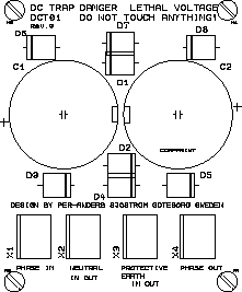
The picture shows the component print of the PCB. Of course you can't use it for anything except for an overview. Please download the pdf-file instead if you want to see the details.
TThe printed circuit board is made of 95 um thick copper. As you can see at the picture the pcb will be at mains potential and therefore lethal. You must insure that this pcb is well protected against unintentional touching. All parts are dangerous to touch when the mains is on..
The component side

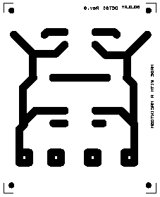
The solder side

The picture shows the component side of the PCB. Of course you can't use it for anything except for an overview. Please download the pdf-file instead if you want to see the details.
Most of the traces are on the solder side.
Technical data


