QSXPS - Regulated Power Supply
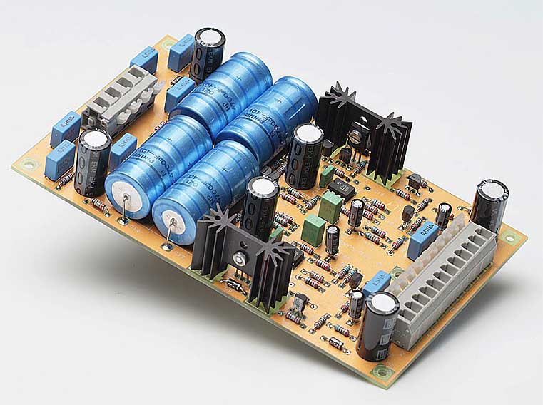
Trivia: Photo taken with a Hasselblad camera with a digital backplane in 1996 (I think). Photographer unknown but used to work for www.elfa.se.
This power supply design did I make for the DAC and for the new ultra extreme RIAA which never left the design stage (maybe it will some day). This power supply gives power to my DAC's almost every day since 1995! Good quality, isn't it? I'm very proud of it and it is not an overkill, like the RIAA amp.
In fact the design is very sensible. No expensive or extreme parts are used and the performance is quite outstanding! If you look at technical data maybe you agree. But remember one thing: This power supply is designed to work with known loads.
It was very fulfilling to have full control over the design process. All parameters are determined by passive components only. I have tailored every detail in the performance. Every part in the power supply have been thoroughly analyzed and tested.
The design
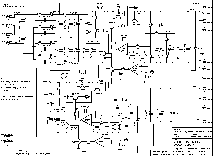
Click on the picture to get a larger view.
The picture shows page 1 of the schematic. Of course you can't use it for anything except for an overview. Please download the pdf-file instead if you want to see the details.
The design is rather unconventional but not very complicated if the different sections are identified. It has similarities with the Jung Super Regulator (as it has been called lately by the diy people) but was designed long before Walter Jung published an article in Audio Amateur, issue 1 and 2, 1995.
The major difference is that the opamp gets it's power from the unstabilized side and the smoothing capacitance is huge, 470µF for an opamp which consumes 2 mA. This design requires opamps which are "rail-to-rail" or almost which LM258/LM358 is. This is crucial at startup. The LM258/LM358 can handle signal near the negative supply pin, pin 4 but not very well signals at "top". Luckily the opamp can start, especially with help from the startup circuit.
Attention to the design note in schematic to the left. There are two resistors which have to be connected differently. See the pdf file.
The PCB layout
The component print
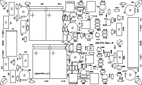
The picture shows the component print of the PCB. Of course you can't use it for anything except for an overview. Please download the pdf-file instead if you want to see the details.
The printed circuit board is made for one or two channels if you use it for QSX Mark II. It's possible to do this pcb by yourself. Just make the layout as the schematics. The pcb have groundplane on the upper side which is essential in order to get good results but you can omit it if you want.
The solder side
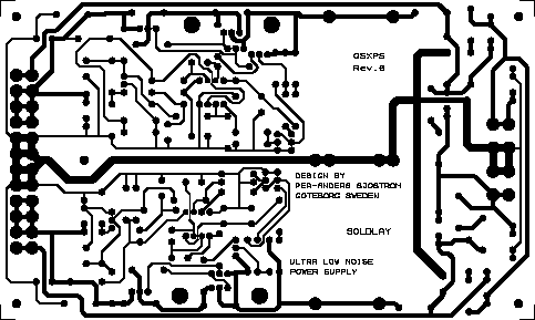
The picture shows the solder side of the PCB. Of course you can't use it for anything except for an overview. Please download the pdf-file instead if you want to see the details.
Everyone of the traces are on the solder side. The groundplane is very covering, no traces on the component side.
The component side
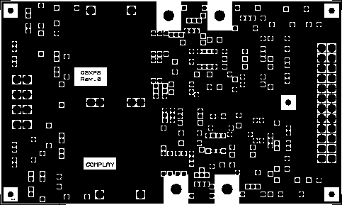
The picture shows the component side of the PCB. Of course you can't use it for anything except for an overview. Please download the pdf-file instead if you want to see the details.
Everyone of the traces are on the solder side as you can see. The groundplane is very covering, no traces on this side.
Technical data
| Output voltage: | +-15 V, +-0,001 V |
| Max output current: | +- 300 mA |
| Output impedance: | 10 micro ohms |
| Hum and noise: | 16 uV at full output current |
| Dimensions: | 101,60 (4") x 170,2 (6,7") mm |
