JSR-01 The Sjöström Super Regulator
Click on the pictures to get a larger view.
This design has been known at www.diyaudio.com and elsewhere and it has been bescribed thoroughly in couple of articles in The Audio Amateur and also in other magazines, like EDN. The design presented below is a developed/altered version (not necessarily better) and not identical to the one in the articles nor to the pcb from Audio Express. Some of the changes has Andrew L Weekes done and some have I done.
Interesting features
- Extremely low noise.
- Very low output impedance in the audioband.
- Small.
- Easy to change voltage, also to negative voltage.
- Well-known and well-tested in serious applications.
The regulator from 1977
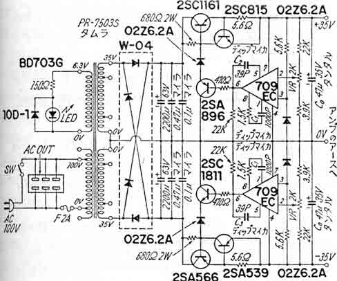
The Super Regulator from 1977, design by Mr. Kaneda.
Let me also point out that the basic idea has been around for at least 35 years. One example can be found in book written by Mr. Kaneda from 1977 and I'll guess he didn't invent it. What has changed since then? The zener references are nowadays much, much better and the opamps are even more much better. In other words there are great opportunities to increase the performance. One more change, rather important also is that the 680 ohms resistor at the top is changed to a constant current generator. This is very important for the output current capability also to the bandwidth, the speed of the regulator.
Is "Super" too much?
Does the design deserve the epithet "super"? Yes, indeed! Can anyone come up with any regulator with less noise and lower output impedance? I don't think so. I would be happy if someone can prove me wrong. This design is extreme in the true sense when it comes to these two parameters. I believe that a couple of more parameters also are state of the art.
I think this design is very interesting from an engineering point of view, a challenge to make it as good as it can be. Therefore I have decided to have it for spin. Since I really like SMD will this be a very "narrow" project, narrow because of the SMD technology. One way to make it a little bit more popular is to gather a bunch of people so I can without risk order rather many pcb's. 61 pcb's were ordered and are now also delivered but according to investigation much later, noone did build. Was it too hard or was there no need for it? Since then a couple has been built though with very good results.
This group purchase was discussed here. Remember, the deal is closed.
My project is unique in the sense that there exists only pcb's with hole mounted parts. This is the first DIY SMD Super Regulator which has left the computer.
Andrew L Weekes ALW has made a very good hole mounted pcb together with a very good documentation. He has also had a group purchase run and he came up with 700-800 pcb's! This shows very clearly the distribution between hole mounted pcb's and SMD pcb's.
There are also a couple of commercial sources, really expensive ones.
The design
The design is based nearly to 100% of the original super regulator. My contribution is transferring it to SMD and making the pcb universal negative/positive versions. I have also made options for three different references.
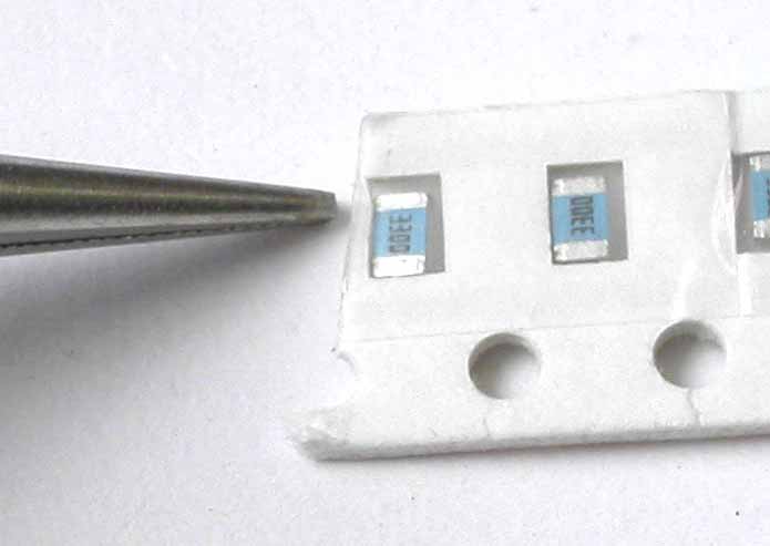
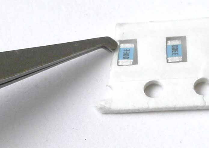
This project is suitable for a newbeginner ONLY if you are handy with the soldering iron AND have the right tools. If you have a soldering iron with small tip and a good pair of tweezers it shouldn't be a problem. I'm going to write down good tips about soldering and mounting parts. This isn't obvious for a newbeginner.
I say it again that SMD is frightening for most DIY'ers and to succeed you must have a good soldering technique and you must also be able to keep a very good order with parts because some of them are unmarked and/or very hard to identify if they are taken from the tape or out of the plastic bag.
The schematics
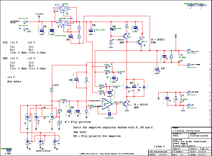
Click on the picture to get a larger view. The picture shows the schematics of the amp. Of course you can't use it for anything except for an overview. Please download the pdf-file instead if you want to see the details.
I recommend that you download the schematics and print it so you can follow the describing text more carefully.
Circuit description
The pre-regulator
The first part is the pre-regulator, IC1 (or IC2) which has a rather odd connection. The sensing network, R1 and R2 is not connected to ground as usual. It's connected to the output so the LM317 regulates the voltage across the pass transistor T2. The purpose of this is to create a constant voltage drop over this transistor. With this connection you will get a more flexible minimum input voltage which is 2.5 volts (according to the values of R1 and R2) plus the minimum voltage across the LM317 which is 2-3 volts. In total you will need approx. 5 volts more than the regulated output voltage.
The main purpose of this regulator is to increase the power supply rejection ratio, PSRR. If you of some reason don't want this pre-regulator just omit, C1-C3, R1, R2, IC1 (or IC2). Solder in a wire between Vin and Vout. See the schematics. The rest of the regulator consists of a reference of some sort, opamp, output stage and feedback network.
The reference
As reference I have chosen to have maximum flexibility. Virtual any reference will fit as long as the voltage is above the common mode limit for the used opamp. 2.5-7 V will work and in some cases also 1.2 V. The original LM329 can only be delivered in TO92 package and not in any kind of SMD. Therefore I have made options for TO92 (hole mounted), SO08 and SOT23. I have used LM431 in SO08 and this very cheap reference is rather good, although not as nearly as good as LM329 but much, much better than a regular zener diode (which also can used). As a little help if you use LM431 hole mounted, I have written down a small note at the pcb, just under C7. It says 431/RAC which is the pinning, Ref, Anode, Cathode. You will have to twist the LM431 in order to fit. No reference can be used for negative voltage just by turning them around or something so therefore all three types are doubled for negative voltages. Please notice that the resistors which are setting the reference voltage must be interchanged, R4 and R5 swap it's positions for negative voltage. R3 is carefully selected and may be changed if especially lower voltages are to be chosen. See instructions for this.
If you want to trim the reference voltage just change R5. If you want exactly 15 volts out, you should have slightly under 5.0 kohms. You could either have 5.1 kohms of solder in one 56 kohms on top of the R5. I chose 5.6 kohms because it's a more common value.
The reference voltage is filtered by R6 and C7, C8 in order to remove the noise and as a side effect you will get a smooth startup. R6 should optimally be R7 and R8 in parallel but I consider this not extremely important. You can either choose 499 ohms or simply solder two 1 kohms on top of each other. If you have matched input impedance's you will minimize the input offset and also the drift with temperature (not very important in audio applications). It may also be good when it comes to common mode rejection. Since the whole design is placed on a groundplane I gather that high frequency problems are not so big so you must take this into account. R9 and C9 are parts for "just in case", to tailoring the frequency properties. Normally R9 is only a tin jumper and C9 is omitted.
The opamp
The opamp can be almost any type as long it's not too fast, faster than the output stage. The maximum speed of the opamp at unity gain is around 30-40 MHz. The AD825 has the bandwidth of 34-37 MHz at unity gain and the AD797 has unity gain bandwidth of approx. 30 MHz. If extremely low noise is important AD797 might be suitable but if "low" noise is sufficient I think any good audio opamp will do, like AD8610, OPA134 etc. Even good old NE5534 may work but I haven't tested this opamp. The only thing you must think of is the common mode limits for the inputs of the opamp. At start-up it's important that the opamp has predictable behaviour, especially sensitive is this for a negative regulator.
At the moment only AD797 and AD825 are tested for 5-14 volts, both positive and negative output voltages.
Power for the opamp
Since the pcb is made both for positive and negative voltages the opamp must have different connections for the power supply voltage, pin 4 and 7 at the opamp. You can either take the power from the output or before the pass transistor T2. What you choose is dependent of used opamp and how low the minimum supply voltage is (see the datasheet for this parameter). Minimum voltage for AD797 is 10 volts so if you want to be really sure you must feed it from the unregulated side if you want less than 10 volts out. Parts which are involved in this are R10-R13 and C10, C11.
Positive regulator, power from the output
R12 = 47 ohms
C11 = 100 nF
C10 = Tin jumper
Negative regulator, power from the output
R11 = 47 ohms
C10 = 100 nF
C11 = Tin jumper
Positive regulator, power from the unregulated side
R13 = 47 ohms
C11 = 100 nF
C10 = Tin jumper
Negative regulator, power from the unregulated side
R10 = 47 ohms
C10 = 100 nF
C11 = Tin jumper
The feedback network
The feedback network is very simple, only R7 and R8. C6 reduces the output impedance half of it's the value. This capacitor is hardly necessary in real life but if you want lower output impedance you should use it. The values of the feedback resistors should be a low as possible considering the max power dissipation. It serves to purposes. The first is to create a voltage divider with good high frequency properties (avoiding unstability) and also to draw current out of the pass transistor, T2. If current flows all the time also the output impedance can be kept low. It's also important for stability reasons.
The output voltage is determined by the reference voltage * (R7/R8 + 1)
The output stage
The output stage is rather unusual. Normally you have only one emitter follower, maybe together with a driver transistor forming a Darlington transistor. This type of output stage is rather slow, too here. To speed things up the driver transistor is changed to a class An emitter follower as the driver for the pass transistor. The load of the emitter follower (T3) is a current source formed by a reference voltage, the LED H1 (makes a nice glow) and R14 together with T1. The current through the LED should be 1-3 mA. If you want very low voltages you must change the value of R14.
The driver is also a bit backwards. This creates a very special and also very important feature, the possibility to a safe power up of the opamp. The output stage deliver max output voltage when the opamp is inactive. This makes the opamp come alive. The zener DZ1 (or DZ2) increases the startup voltage and creates also a necessary DC shift so the output of the opamp works at ideally at half the output voltage. This zener voltage must be decreased when lower output voltages are wanted. For 5 volts it's sufficient with a diode in the forward direction, creating only 0.7 volts. T3 is added compared to Walt Jung's original (but Mr. Kaneda had it) and unloads the opamp from the drive currents. C12 takes down the impedance of the zener.
No short circuit limiting
I have increased the current of the driver T1 and T2, for higher speed but this makes also the regulator more vulnerable against short circuit so I suggest you are careful when you are connecting.
Capacitive load and C13
The faster opamps you have, the more sensitive against capacitive load the regulator will get, meaning low loss capacitive load. The regulator has a minimum load of 0.3-0.5 ohms and if you have a 100 nF connected very close to the output transistor you can get an impedance lower than 0.5 ohms. This frequency will be at 3 MHz. Therefore the C13 must not be too "good". In fact a "normal" cap is sufficient and if you choose a low impedance cap you may experience unstability. If you use a fast opamp, it simulates a cap rather high up in frequency so serious decoupling this close to the output transistor isn't necessary but if you only have 30 mm wire the regulator can take 100 nF or more. The short wire creates a small inductance which is sufficient in order to limit the lowest impedance.
The "sense" connections
The sense connections are a bit overkill but if anyone wants these I have added this feature. The sense function is mainly to subtract or eliminate the losses in the power wires, which won't be especially large. It's just milliamps. If you want this feature make sure that the sense wires are close to the power wires so instability can be avoided. If you don't want to use this feature, just put two tin jumpers, close to the connector (you can't miss it) on the solderside of the pcb. If you are sure that you never will use the sense function you can also omit R16, R17, C14 and C15.
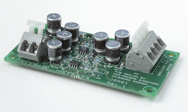
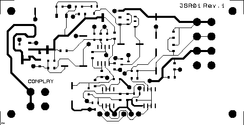
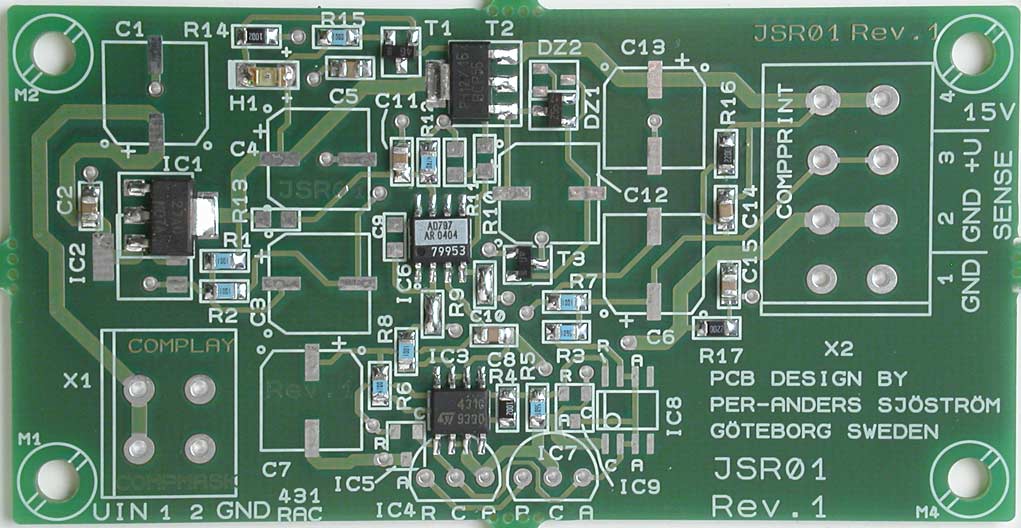
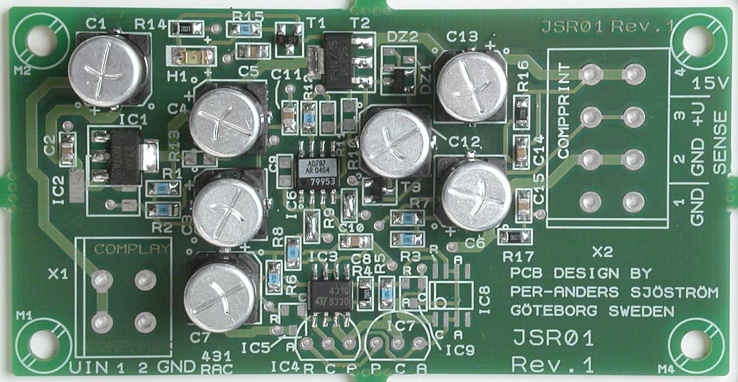
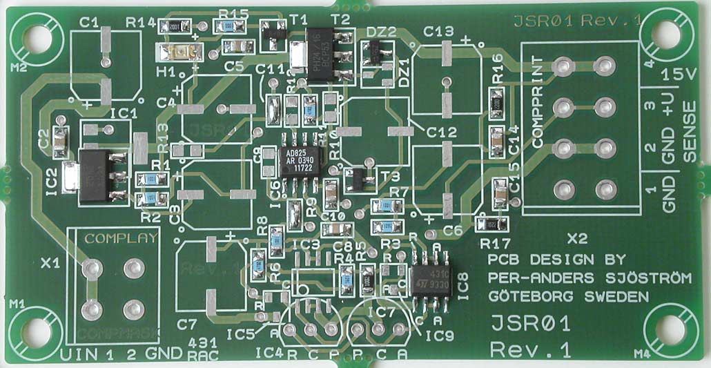
The pcb layout
The component side.
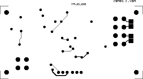
The solder side.
.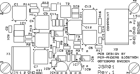
The component print.
The pcb layout is designed so you can build both a positive and a negative version on the same pcb. You must pay extra attention to which parts should be used for each version.
Build directions
Tools
I have two soldering irons, one regular 50 Watts Weller (older model) but similar as WS-51, with a small tip plus a small cute SMD iron, Weller WS-81 with 80 watts of power. This sodering has a very small tip. I use regular 60/40 tin, diam. 0.7 mm. I don't use any solder paste but it's possible. I have also a good pair of tweezers (picture will come), especially made for SMD parts.
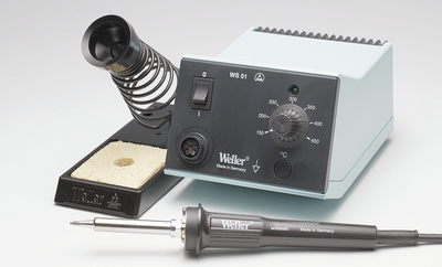
Weller WS-51, 50 Watts, soldering station, general purpose. Photo borrowed from ELFA.
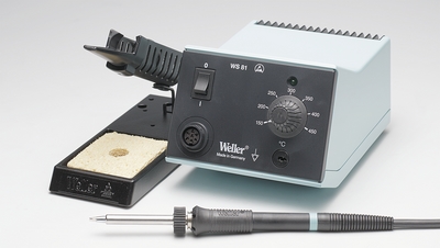
Weller WS-81, 80 Watts, soldering station, SMD usage. Photo borrowed from ELFA.
Those soldering stations are for professional use and are also (therefore) expensive but you must have two things: Small tip and adjustable temperature. If you can borrow and second soldering iron, it's very practical when you shall solder 0805 parts, like resistors and capacitors.
![]()
Click on the picture to get a larger view.
Click on the picture to get a larger view.
This is a good model of you want a powerful tweezer but for holding SMD parts the model below is better.
![]()
Click on the picture to get a larger view.
Click on the picture to get a larger view.
This is a really nice pair of tweezer. Perfect for handling small SMD parts.
....more to come.....
I have taken photos of two basic configurations. Capacitors are removed so you can see the small parts more clearly.
Configuration +14 volt, AD797, pre-regulator
Click on the pictures to get a larger view.
Click on the pictures to get a larger view.
Configuration -14 volt, AD825, pre-regulator
Click on the pictures to get a larger view.

Click on the pictures to get a larger view.
Test
Not much here I'm afraid.....
Technical data
| Operating voltage: | 19-35 V, less current at high voltage in. |
| Output voltage: | 5-30 V |
| Hum and noise at full output current: | Down to 1 µV or below depending of component choices |
| Max current: | Approx. 150mA peak |
| Max continuous current: | Approx. 100 mA depending of ambient temperature and mounting. |
| Dimensions: | 83 (3.3") x 42 (1,7") mm |
