SST-03 The softstart for toroidal transformers
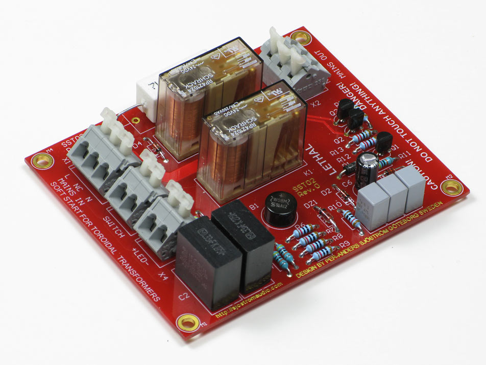
Picture of the pcb. The pcb is doublesided with plated through holes and the copper is extra thick.
WARNING - CAUTION
As you can see at the picture the pcb will be at mains potential and therefore lethal. You must ensure that this pcb is well protected against unintentional touching. All parts are dangerous to touch when the mains is switched on.
Do you have an amplifier with a toroid, 500 VA or more? Do you have problems with burned fuses in the wall? Maybe you also are having trouble with mains switches which don't last long. Maybe this soft start circuit may be something for you. It's easy to build and it's virtually impossible to burn the traces. The pcb has 105 um (3 oz.) copper and is double sided with a professional look and quality.
Interesting features:
- Fast reset time.
- Consumes very little power.
- Very thick copper traces, virtually impossible to burn off.
- No need for high current rating of the mains switch.
- Space for 7 watt resistor.
- Gold plated pads.
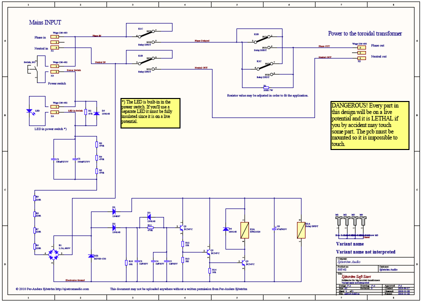
The schematic
Click on the picture to get a larger view. The picture shows the schematics of the amp. Of course you can't use it for anything except for an overview. Please download the pdf-file instead if you want to see the details.
Circuit description
The two functional blocks
The circuit consists of two blocks. Block one is a simple power switch maneuvered by K1 and the other part is the inrush current limiter formed by relay K2 and R1.
The purpose of K1 is to relieve the power switch from the main current and lower the demands of this switch. You can use any switch capable of switching 2 A at 250 VAC (or 110 VAC if you have this AC voltage). If you of some reason don't want to use this feature, just put a wire in X3 and if you don't want a LED indication, put a wire in X4 also. If you do want a LED indication, this LED must be properly insulated because it is floating at main potential and is (may be) therefore lethal to touch. The original idea for the LED idea come from that I wanted to use a switch with built-in LED.
Reliable circuit
This design have I used now since 1989 in the QRO-amp. So the design is well proven. The C1, C2 design is used in time relays and manufactured in millions of copies. I have personal experience of this circuit. More than 10000 units are out and none of them have had any failure of the C1, C2 cap.
Lossless resistor
The power for the electronics is derived through a capacitor which acts like a "lossless resistor". This technique is possible to use if the wave shape of the mains is good enough (sinus with no harmonics). The size of the C1 and C2 is rather critical. If you are going to use 110-120 VAC the capacitance must be double, but this isn't tested yet, the exact value.
Trimming brightness of the LED
R2 is for trimming the brightness of the LED which may be located inside the mains switch. I personally like mains switches with LED's but unfortunately the are rather small, can't handle much current. K1 is used for unloading the switch. A 2 x 5 (8) A relay will last at least 10 years. My have lasted 20 years with a 600 VA transformer. R2 act also as protection for negative voltages across the LED.
Avoiding unpleasant surprises
R3-R5 are for avoiding unpleasant surprises, to discharge the C1 and C2. Three resistors is used to ensure resistance against transients. The total value should be between 220 kohms to 3 Mohms.
Transient protection
R6-R9 limit the max inrush current for C1 and C2. Four resistors are used simply because they are small and cheap.
Creating DC
B1 fullwave rectifies the voltage and is limited by the zener DZ1 when the normal load is small. The zener is hardly necessary since you always have a load in K1.
The C6 should not be too large. Larger capacitors reduces the supply voltage, not the other way around. This is because we have a capacitive voltage divider. C1, C2 and C6 forms a voltage divider.
D1 is for isolating the timing circuit and insure a short reset time.
The timing circuit
R11 and C4, C5 is the timing circuit. R12, R13 makes the time longer. T2 is simply a buffer since K2 consumes rather much current. You can use a small mosfet as T3, BS170 or similar but I have chosen here to only use common parts.
Only C4 gives a sufficient delay time for most situations but the time can be increased by mounting also C5. No harm to have both, but R1 may have to be changed due to extra power dissipation.
C3 is smoothing for the timing voltage and this capacitors should be as small as possible. R10 is a bleeder which discharges the whole timing circuit as fast as possible. The is one of the main features, fast reset time.
Inrush limiter
R1 limits the inrush current. 5 W is enough for at least 600 VA and rather much smoothing. My power supply has 600 VA and 88000 uF, 2 x 63 V, 4 x 22000 uF. Chosen value of R1 gives 3 A as max current. The holes in the pcb are extra large so it's possible to solder in wires and use an external resistor if you have need for it. The holes are 1.5 mm.
Other mains voltages
The pcb is not tested yet for 110-120 VAC but I'll expect that 2 x 0.68 uF (C1, C2) would be sufficient. The capacitor value is also dependent of the relays and their current consumption.
Relay type
I have chosen here an Schrack relay which can handle 8 ampere but I consider Elesta SGR282 24 VDC as one of the best relays there is. It is also rated to 8 ampere. Note also that max switching current probably is very low most of the time because you don't switch off the amp at full power. With this assumption the relay will be able to handle more than 8 A as long it's not switched.
Build directions
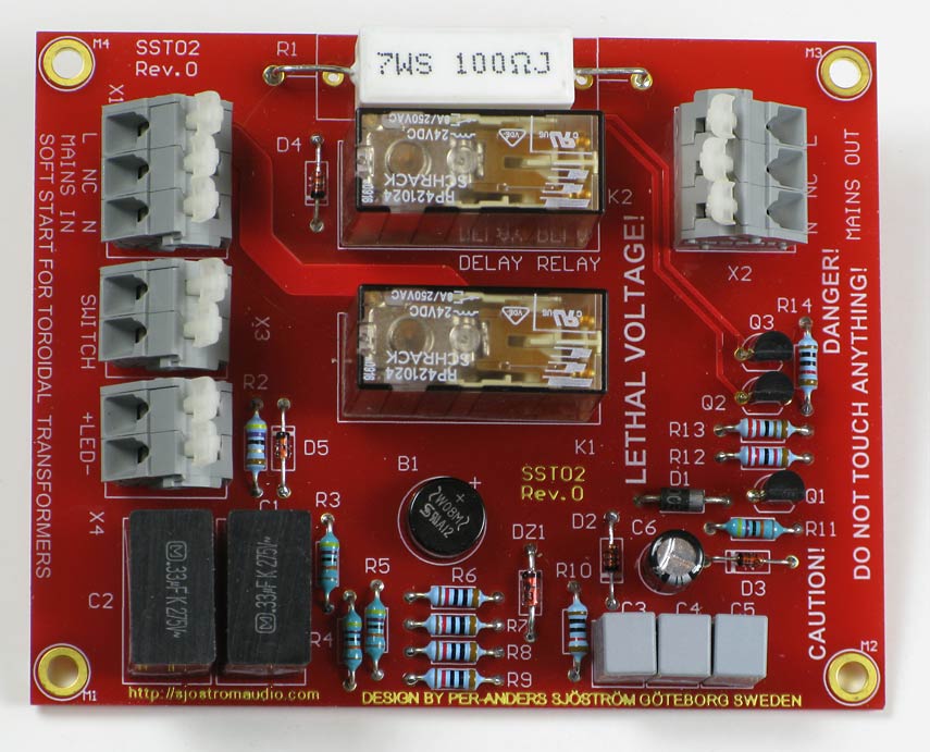
Click on the picture to get a larger view.
This design is very easy to build. You should start with all low parts. Solder in the relays at last.
Soldering
This pcb has very thick copper traces, 95 um. This means that they cool very good. The result of this is cold joints if you don't observe some advice's. The R1, K1, K2, X1-X4 demand very much heat. You must really burn the solder joint for at least 5-10 seconds. Make sure that the tin really melts and becomes shiny and smooth. K1 and X1 have traces on the component side so these parts must be very carefully soldered because you won't be able to inspect the soldering.
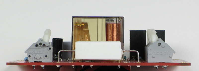
Detail of the series resistor. Click on the picture to get a larger view.
If the resistor gets hot after a start you could mount it 1 or 2 mm above the pcb surface. By this the pcb won't be miscoloured
The pcb layout
Click on the picture to get a larger view.
Please download the pdf file if you want to study the pcb layout.
Test
Click on the picture to get a larger view.
----- Please notice this first!-----------
If you can, use a 24 V DC source to test the time delay function. Apply voltage 24 VDC across DZ1 or any other suitable point. Notice that K1 will activate immediately and the K2 300-600 ms later, depending of if you have both C4 and C5 mounted. Check also that the relay contacts work properly. If it works all right with 24 VDC then test with 230 VAC.
Activation voltages
| 2 x 330 nF, 50 Hz | K1 | K2 |
| Activate (pull-in voltage) | 99 V | 182 V |
| Deactivate (drop-out voltage) | 48 V | 140 V |
| 2 x 680 nF, 50 Hz | ||
| Activate | 48 V | 85 V |
| Deactivate | 22 V | 67 V |
"Activate" means when the relays close their contacts. The values are tested with Omron relay and are approximate. If you choose other relays with different current consumption these voltages will be different.
The soft starter is ready.
Technical data
Click on the picture to get a larger view.
| Operating voltage: | 190-240 VAC, 50 Hz, other voltages and frequencies need some changes |
| Delay time: | 300-600 ms |
| Max inrush current: | Approx 3 A peak |
| Max continuous current: | See datasheet for used relays |
| Dimensions: | 99.1 (3.9") x 78,7 (3,1") mm |


