Page 5 of 10
The pcb layout
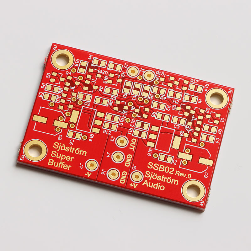
The component side, top side
Click on the picture to see a preview of the pcb.
The printed circuit board is made for one channel. It requires stabilized power supply with ± 12-15 V.
The pcb have groundplane on the bottom side and partly on the top side, which is essential in order to get good results.
Almost everyone of the traces are on the component (top) side. The groundplane on the bottom side is very covering, only a few traces are there.
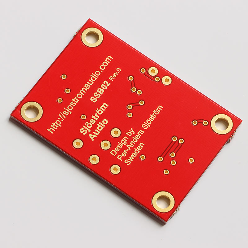
The bottom side
The picture shows the bottom side of the PCB. 95 % or even 99 % is covered with a ground plane and the only thing to solder on this side are the wires.


