QRV-08 The high performance smd headphone amplifier with quadruple super regulators
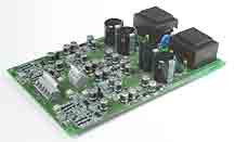
Click on the picture to see a larger view of the pcb.
The performance is outrageous in headphone amp terms. See the technical data!
Interesting features:
- High speed, low distortion current feedback design.
- All discrete design of the amp itself.
- Offset trim with a trimpot and/or with a DC servo.
- Input LP-filter if you have problems with RF interference (you should have a filter though).
- Room for DC removal cap (if you need this)
- High speed and high performance SMD buffer as output stage.
- High current transistors as output stage.
- Extremely high quality dual mono power supply with large smoothing caps and transformers on the pcb and with four extremely high speed and high performing super regulators.
- Fits any headphone (except for electrostatic of course).
- Any bad feature? Possibly that this project requires skills more than usual in order to succeed. The skills are about soldering the parts in the right place. If you'll manage that, this isn't so hard after all. Building time 4-6 hours only.
My design goal was to make an ultra high performing amp with only "normal" parts but well balanced amp in terms of component choices and a well-tested topology. I think I have succeeded because this design is one of the best I ever have done so far and I'm pretty sure that the power supply is one of the most advanced regardless of price in commercial products.
The background
This project is not suitable for a newbeginner, but if you only have a soldering iron with a very fine tip and you don't tremble and have a good pair of tweezers, it shouldn't be any problems to succeed. This amp is not very hard to solder, yes I'm not kidding and it's really cool, not common DIY stuff!
I have made this amp purely for my own pleasure but if someone wants to build it (and is skilled enough), please go ahead. This type of amp is very fast, by nature. The amp consists of three main blocks, input buffer, the amp itself and the output buffer is called "diamond buffer" but I don't where the name comes from. I have also seen the name "Jung Super Buffer" (from his article). Many IC's have this diamond buffer LT1223, BUF634, LME49600 and many more.
This headphone amp can also be used in a preamp as line stage with or without gain, as buffer for DAC's and CD-players.
There are lot's of good info out there on this subject buffers and current feedback amps. Walter Jung has written a couple of good articles and one of them is about this particular buffer. In fact his article is THE best for a normal DIY'er. See references here.
Since many years back I make SMD designs at work so I know about the good properties. One of the real important benefits are the compactness and the good HF performance. You'll get good performance of the passive parts way above 100 MHz and this ensures extremely high performance in the audioband. A man from Slovakia has done some measurements and they indicate distortion numbers down to 0.00046%! Incredible, isn't it, with a design consisting of 2 cents transistors! I can confirm that the performance is way better than my soundcard, 0.0078%.
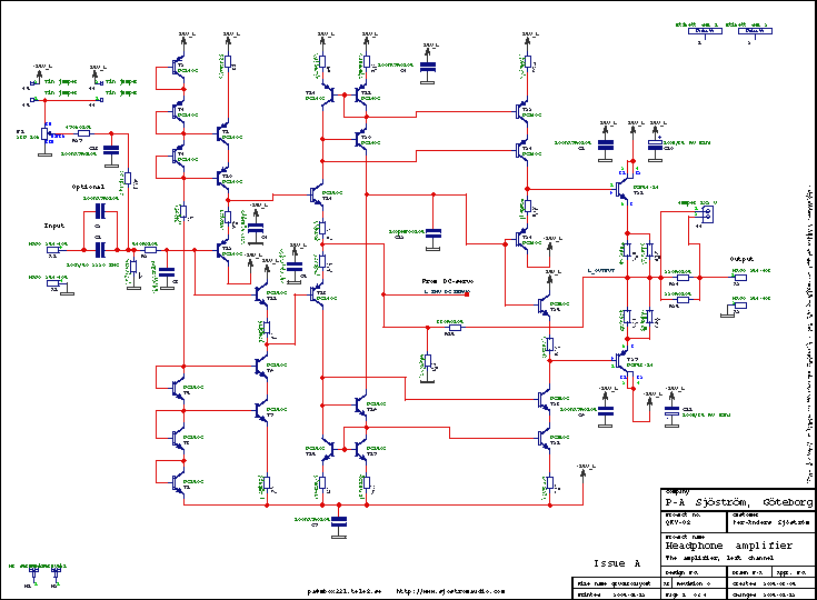
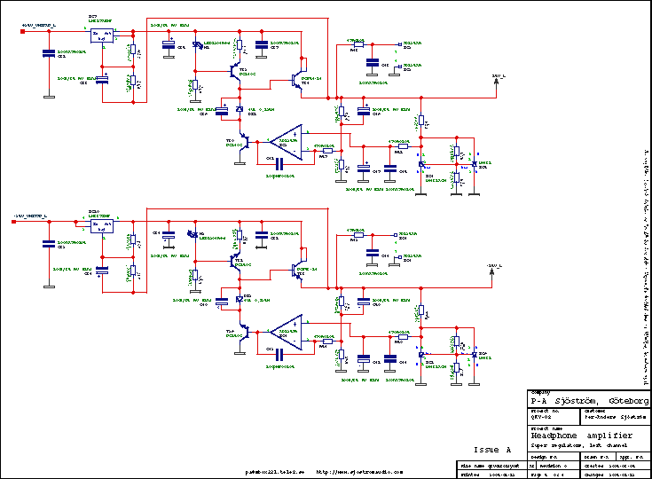
The schematics, page 1 and 2.
Click on the picture to get a larger view. The picture shows the schematics of the amp. Of course you can't use it for anything except for an overview. Please download the pdf-file instead if you want to see the details.
The text is for the right channel.
I have chosen to use current generators with cascodes as emitter loads. How much good the cascodes do is unknown at the moment. The only obvious disadvantage is a little bit reduced output voltage swing, otherwise only positive things, like less distotion and higher speed.
The current in the first stage (the input buffer) is set by T1, T3 and T2, T4 along with R4 and R5. I have transistors as diodes just to make it simpler when it comes to parts. The current is 0.65/560= 1,1 mA. The input stage of the amp is set by the relationship between R6/R10, and R7/R11, 10/2.2 = 4.5 => 5.3 mA. This current is then mirrored in the wilson current mirror, formed by T16, T18, T20, R8, R12 and T15, T17, T19, R9, R13. The resistors serves as local feedback which make the currents mirrors a little bit more linear.
The collectors of T19 and T20 creates a high impedance node and is also the output of the amp. This high impedance output must be buffered in order to useful. This is done with a diamond buffer. The current is given by the current in the mirror times R12/16 = 2.4 mA. The output stage runs in class A (which the whole amp does) 2.4 mA * R18/(R20//R22) = 10.2 mA.
My choice of currents is "average", because you both increase them och also decrease them. The max current is set by the max allowable power dissipation of the transistors. The small SOT23 types can take 310 mW or so and the SOT223, output transistors can dissipate 1.3 W but not in this application I imagine. More current mean slightly higher speed.
The input filter R2, C3 may be necessary if you are having trouble with RF interference. The values can be set to almost anything. The frequency is calculated by f= 1/(2*pi*R2*C3).
The performance is very good. See the technical data!
Interesting features:
- The pcb fits virtually any SOT23 small signal transistor and almost any SOT223 power transistor.
- The emitter loads have cascodes in order to increase linearity.
- SMD caps, including electrolytic caps.
- SMD parts which makes the buffer very small and thin.
- Input LP-filter if you have problems with RF interference, if not just omit it.
- Professional pcb with groundplane which establish good cooling and shielding.
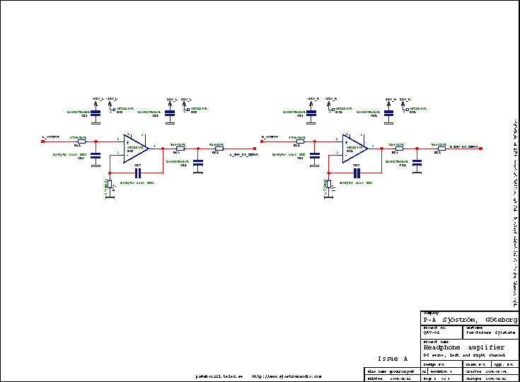
The schematics, page 2
Click on the picture to get a larger view. The picture shows the schematics of the amp. Of course you can't use it for anything except for an overview. Please download the pdf-file instead if you want to see the details.
This is the DC-servo which is non-inverting and is a well-known design.
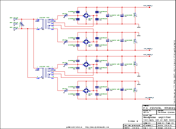
The schematics, page 4
Click on the picture to get a larger view. The picture shows the schematics of the amp. Of course you can't use it for anything except for an overview. Please download the pdf-file instead if you want to see the details.
These pages show the design for the raw voltage. R58 is a varistor and is for supression of high voltage spikes.
The schematics, page 5 and 6.
Click on the picture to get a larger view. The picture shows the schematics of the amp. Of course you can't use it for anything except for an overview. Please download the pdf-file instead if you want to see the details.
The regulator topology is called "super regulator" because of it's super performance. Please see my SSR01 for more info.
The pcb layout
The component print
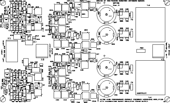
The picture shows the component print of the PCB. Of course you can't use it for anything except for an overview. Please download the pdf-file instead if you want to see the details.
The printed circuit board is made for two channels, contains everything, power supply and the amp itself, including transformers except for input and output connectors. I have chosen not to have pcb mounted headphone and phono connectors because it's hard to fit in a case.
The pcb have groundplane on the lower (solder) side (not shown in pictures) which is essential in order to get good results.
The solder side
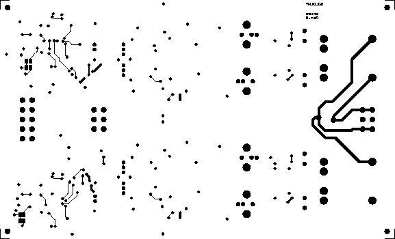
The picture shows the solder side of the PCB. Of course you can't use it for anything except for an overview. Please download the pdf-file instead if you want to see the details.
Almost everyone of the traces are on the solder side. The groundplane is very covering, only a few traces on the solder side.
The component side
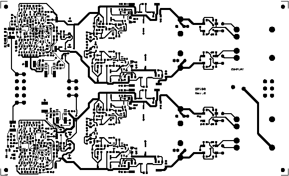
The picture shows the component side of the PCB. Of course you can't use it for anything except for an overview. Please download the pdf-file instead if you want to see the details.
Almost everyone of the traces are on the component side as you can see. The groundplane is on the solder side.
The groundplane mask

The picture shows the groundplane mask of the PCB. Of course you can't use it for anything except for an overview. Please download the pdf-file instead if you want to see the details.
The black area is without groundplane and this is under the transformers.
The hot relief pads
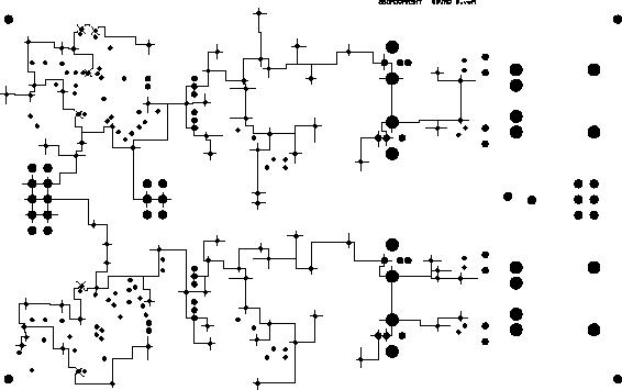
The picture shows the pads which are connected to groundplane of the PCB. Of course you can't use it for anything except for an overview. Please download the pdf-file instead if you want to see the details.
Each "cross" at the pads is a ground connection. This file is used together with the solder side in a sandwich. I use this technique because my cad program has a very slow groundplane generation.
Build directions
Click on the picture to see a larger view.
This design is very easy to build. You can of course solder everything and then apply voltage but maybe it doesn't hurt to be a little cautious. You should start with all low SMD parts except for the buffer and the opamp becuase it's harder to solder the SMD parts when you have big parts in the way. For this solder job I recommend a good pair of tweezers. I use a type especially made for SMD. With this tweezer I get a very good grip. You must also have a soldering iron with a small tip but at least 50 watts in order to be able to solder the buffer which requires lot's of heat.
Start with all low SMD parts except for buffer and opamp.
- Resistors
Transistors
Trim pot (if you use it)
Capacitors, not the hole mounted ones
Rectifier bridges, at last - Then continue with the high electrolytic caps, mount all caps
- Connectors
- Jumpers
- Transformers
- Varistor
Good luck and happy listening.
Listening experience
How does it sound really? The prototype is built and it works real good.
This is the best design I ever have done. I'm really pleased.
It's totally transparent, like a polished diamond with a dry analytical sound, no colouration what so ever. Very revealing though. You must have good recordings because nothing is hidden. All is the there including noise, breathtakes from the musicians, noise from the ventilation, sounds from the instruments besides the tones.
I'm also very influenced by the looks. I really like SMD. It's very cute, don't you think?
I think I'm influenced of the pure and technical clean electrical performance. Step response is excellent and the offset voltage is extreme!
Technical data
Measurements done by jmd01 from Bratislava, Slavakia
Excellent measurements done by Neurochrome. Many thanks, Tom!
| Frequency response: | 0 Hz - 25 MHz(?), more than 10 MHz. This is valid without input coupling cap. With this cap, 8 or 17 Hz |
| Frequency response with input filter: | 0 Hz - 1.29 MHz, -3 dB. This is valid without input coupling cap. With this cap, 8 or 17 Hz |
| Power bandwidth at 7 Vrms, 50 ohms: | 0 Hz - 25 MHz(?), more than 10 MHz. This is valid without input coupling cap. With this cap, 8 or 17 Hz |
| Equivalent input noise: | 0,6 µV |
| Signal to noise ratio: | 112 dB at 1 V out |
| Dynamic headroom: | 129 dB |
| Distortion: | 0,00042% |
| Slew rate: | 1200 V/us |
| Step response: | Perfect without overshoot |
| Gain: | 4 (12 dB) |
| Input impedance: | >1 Mohms, pullup, pulldown resistors not included. |
| Output impedance: | 2.5 ohms |
| Output current: | 120 mA peak |
| Supply voltage: | 230 VAC in, 115 VAC is also possible. |
| Dimensions: | 203,2 (8,0") x 123,2 (4,85") mm |

