QRV-07 - The ultra high performance SMD headphone amplifier
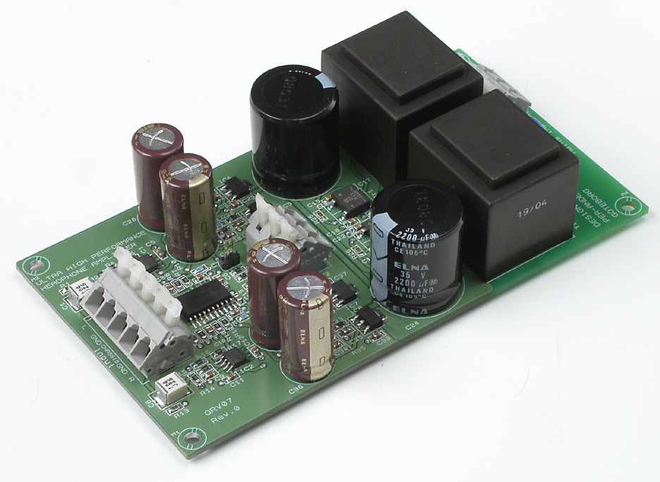
Click on the picture to see a larger view of the pcb.
The performance is outrageous in headphone amp terms. See the technical data!
Interesting features:
- The pcb fits virtually any single opamp
- Room for good coupling caps (if you must or like).
- Input LP-filter if you have problems with RF interference (you should have a filter though).
- High speed and high performance SMD current feedback amp as output stage.
- No global feedback.
- High quality power supply with large smoothing caps and transformers on the pcb.
- Separate voltage regulators for each channel.
- Fits any headphone.
My design goal was to take out most of the performance of the TPA6120 and when I listen to the amp I think I have succeeded.
The background
Click on the picture to see a larger view of the pcb.
This headphone amplifier is based on the extremely high performing TPA6120. I saw this IC some time ago and I was very astonished by the extremely low distortion figures 0.000021% and the extreme speed, 100 MHz. Observe the zeros in the distortion figures! I don't think I have seen anything lower. Remember though that distortion figures aren't everything but high speed is always good and certainly in combination with low distortion. Based on these facts I have decided to let this headphone amp IC have a go.
This project is not suitable for a newbeginner, but if you only have a soldering iron with a very fine tip and you don't tremble and have a good pair of tweezers, it shouldn't be any problems to succeed. This amp is not very hard to solder, yes I'm not kidding and it's really cool, not common DIY stuff!
Notice that TPA6120 has a very special package which may be a bit hard to solder. See my instructions about this.
The package is called PowerPAD and more info about this is found here.
Quote from Texas Instruments:
The PowerPAD thermally enhanced package provides greater design flexibility and increased thermal efficiency in a standard size IC package. PowerPAD's improved performance permits higher clock speeds, more compact systems and more aggressive design criteria.
PowerPAD packages are available in several standard surface mount configurations. They can be mounted using standard printed circuit board (PCB) assembly techniques, and can be removed and replaced using standard repair procedures.
To make optimum use of the thermal efficiencies designed into the PowerPAD package, the PCB must be designed with this technology in mind. This document will focus on the specifics of integrating a PowerPAD package into the PCB design.
This is what Texas Instruments wants to say about their new ultra extreme headphone amp IC.
The TPA6120A2 is a high fidelity audio amplifier built on a current-feedback architecture. This high bandwidth, extremely low noise device is ideal for high performance equipment. The better than 120 dB of dynamic range exceeds the capabilities of the human ear, ensuring that nothing audible is lost due to the amplifier. The solid design and performance of the TPA6120A2 ensures that music, not the amplifier, is heard.
Evaluation module
Texas Instruments has made an evaluation module which can be bought for a rather cheap price. This module has a good documentation which can be found here.
Active elements are AD8610, OPA134 or OPA627 and a headphone amp TPA6120. The operational amplifiers are one of the best in their market segments. The AD8610 is new and very interesting and I have chosen this to be my reference opamp. Any high performing opamp
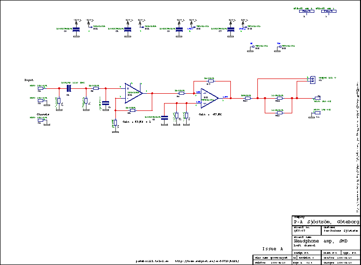
The schematics, page 1 and 2.
Click on the picture to get a larger view. The picture shows the schematics of the amp. Of course you can't use it for anything except for an overview. Please download the pdf-file instead if you want to see the details.
The text is for the left channel.
The main part is a power amp, the TPA6120, IC3. The TPA6120 is a new headphone amp IC with extra good driving capability of 700 mA which will be sufficient for all headphones on the market. The TPA6120 is of a current feedback topology and this makes the inputs a bit unusual. The input bias currents are around 12 µA which more or less means that you must use a buffer in front of the TPA6120. This IC is designed to be used with low impedance signal sources so in order to avoid problems I have chosen to let an AD8610, IC1 feed the TPA6120.
Inverting mode for the TPA6120
The TPA6120 runs in inverting mode just because this will reduce the distortion by a factor of 10. This means that this design will invert the signal. Some people have problems with that but the only way to circumvent this is to use Sennheiser headphones with separate cables. Sorry believers for the absolute phase, this is not a product for you. Still it isn't totally impossible to change the amp to a non-inverting one but it requires a bit handiness. I leave this to those who are mighty for the task.
The input buffer
This design needs an input buffer because of the rather high input bias currents of the TPA6120. I have chosen AD8610 just because I like it. Any good single SO08 opamp will do here.
The gain
The total gain is determined by R4 and R5. Gain = R5/R4 + 1. Low values of these resistors is important if you want low noise.
The output has R10 and R11 in parallel with R12 this serves to purposes. The first one, R10 is to let the TPA6120 feel a pure resistive high frequency load or simply isolate the amp from capacitive load. R11 and R12 is common practice to interface normal headphones. Without these resistors it's very easy to damage low impedance headphones but if you have full control over the situation, omit those resistors, use the jumper J1. I should mention that many headphones are designed to be driven from a certain source impedance. Some people claim that this impedance is 120 ohms. Test this if you want to optimize the listening experience.
The input filter
The input filter is very universal. You should have a lowpass filter, R3 and C3, but if you don't have any RFI trouble at all, it's not necessary, just replace the R3 with a jumper and omit C5. DC blocking capacitor may be necessary but check with your signal source first. The whole amp is DC connected so you must ensure that you haven't got any DC in your signal. The resistor R2 creates a DC path for the inputs of the opamp, otherwise it won't work. R1 is a pulldown resistor so the input coupling capacitor won't pick up any charges when the amp is unconnected. A charged capacitor can create a nasty spike at the output when something is connected to input.
The output power amp
The output power amp is the TPA6120 and is a current feedback type. I gather it's similar to my QRV-06. I recommend some reading in the datasheet of this very exciting IC. It's obvious that this extremely fast IC not is suited for anything else than a high quality printed circuit board. This pcb which I have made has double groundplanes, both to ensure good HF properites and also goos cooling.
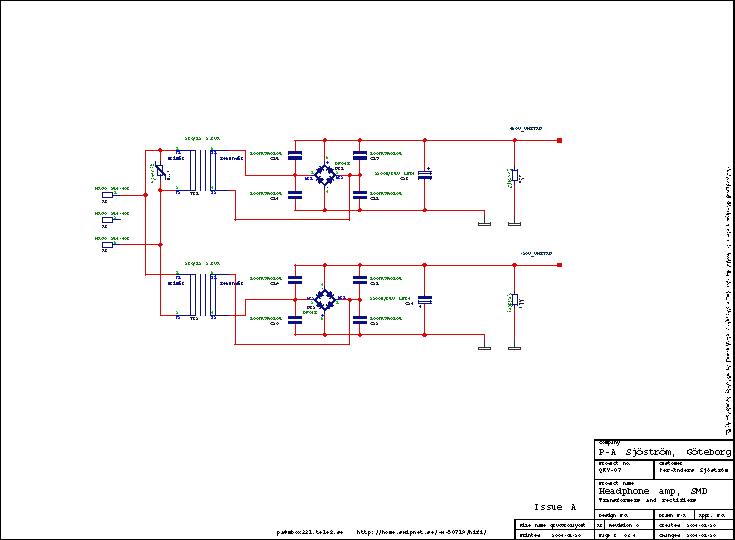
The schematics, page 3
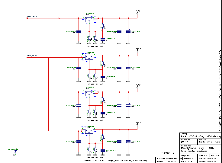
The schematics, page 4
Click on the picture to get a larger view. The picture shows the schematics of the amp. Of course you can't use it for anything except for an overview. Please download the pdf-file instead if you want to see the details.
The power supply is not very exotic, rather straight forward. It's designed to use two transformers, one for the positive voltage and the other one for the negative. I have also used the option to have separate regulators for each channel. It may add some positive effects but I don't know how much. The TPA6120 has an option for separate power connections so why don't use it? Those regulators are cheap and it certainly can't hurt.
The regulators are cooled by the groundplane and of a copper area on the upper side. Practical tests have shown that it works pretty good. The amp is warm, not hot in hard usage.
R25, R26 are bleeder resistors. The regulators won't discharge the capacitors completely when the have reached the voltage of 0,6 V. The resistor creates a clean start at power up.
C15-C18 are for reducing EMI caused by diode switching.
The transformers are short circuit proof by design, therefore you don't need fuses.
R39 is for transient suppression.
The pcb layout
The real life pcb
Click on the picture to see a larger view of the pcb.
Click on the picture to see a larger view of the pcb.
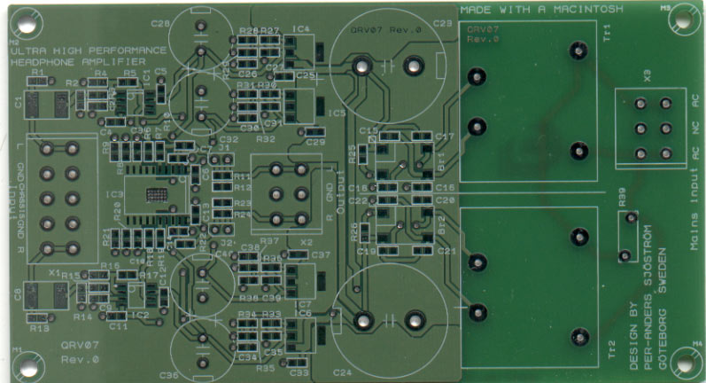
The component print

The picture shows the component print of the PCB. Of course you can't use it for anything except for an overview. Please download the pdf-file instead if you want to see the details.
The printed circuit board is made for two channels, contains everything, power supply and the amp itself, including transformers except for connectors. I have chosen not to have pcb mounted headphone and phono connectors because it's hard to fit in a case.
The pcb has groundplane on both sides (not shown in pictures) which is essential in order to get good results.
The solder side
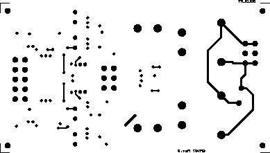
The picture shows the solder side of the PCB. Of course you can't use it for anything except for an overview. Please download the pdf-file instead if you want to see the details.
Almost everyone of the traces are on the solder side. The groundplane is very covering, only a few traces on the solder side.
The component side

The picture shows the component side of the PCB. Of course you can't use it for anything except for an overview. Please download the pdf-file instead if you want to see the details.
Almost everyone of the traces are on the component side as you can see. The groundplane is both on the solder side and the component side.
Build directions
Click on the picture to see a larger view of the pcb.
This design is very easy to build. You can of course solder everything and then apply voltage but maybe it doesn't hurt to be a little cautious. You should start with all low SMD parts except for the output power amp and the opamp because it's harder to solder the SMD parts when you have big parts in the way. For this solder job I recommend a good pair of tweezers. I use a type especially made for SMD. With this tweezer I get a very good grip. You must also have a soldering iron with a small tip but at least 50 watts in order to be able to solder the buffer which requires lot's of heat.
Start with all low SMD parts except for the output power amp and the opamp.
- Resistors
Transistors
Trim pot (if you use it)
Capacitors, not the hole mounted ones
Rectifier bridges, at last - Then continue with the high electrolytic caps, mount all caps
- Connectors
- Jumpers
- Transformers
- Varistor
Apply voltage, 230 volts AC. Check that the regulators give the expected voltage, +- 12 volts. Disconnect the power and see to that the voltage is zero when you continue the soldering.
Continue with the opamp and output power amp.
- Opamp.
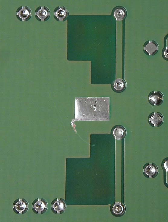
- Output power amp. This part needs to be soldered into the large pad on the pcb. To do this you must use lot's of heat. If you have two soldering irons, use both at the same time. The buffer gets it's cooling via this pad so it's important that the buffer is very good soldered. When I soldered this IC, it turned out not to be so difficult. Solder the pins as usual. Then solder the backside. Turn up the soldering iron to max temperature, like 450 deg C in my case. Warm and add tin and continue to warm for 10-20 seconds or so. Notice how the tin gets sucked up through the via holes. You can "burn" quite a lot and the upper side won't melt.
Click on the pictures to see a larger view of the pcb.
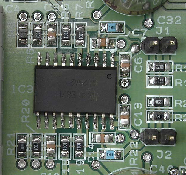
Detail of the TPA6120 and how it's soldered. Notice the 18 vias under the IC which serves as heat transport.
Check the finished amp
Apply voltage again and check the output voltage. Measure the DC voltage at the output. It should be the specified offset voltage (see datasheet) and times the gain, 4 in this case. I got 78 uV(!) for AD8610 and 2 and 10 mV for the TPA6120 at the amp outputs. 10 mV is OK and won't harm the headphones.
The whole amp is ready.
Test if you want the different drive modes. It is safe to change modes when voltage and input signal is applied. You won't even hear a click.
Good luck and happy listening.
Listening impressions
Click on the picture to see a larger view of the pcb.
How does it sound really?
First impression is really, really, really good. The second impressions are even better. This amp is crystal clear with extremely well controlled behaviour. "s"-sounds sounds excellent, tight bass, warmth in the mids. This headphone amp may be the best in the world? And the best of all: The parts aren't particulary expensive!
I have made a simple distortion measurment with the excellent russian freeware Rightmark Audio Analyzer. What we can see is that the amp is better than the sound card I have used.
Read what Suzy thinks:
The beginnings of a new amp to drive my Sennheiser HD595 headphones. I was greatly impressed by the TI TPA6120 current mode feedback headphone amp chip, with incredibly low distortion levels. I began designing a board to try one out, but found almost exactly what I was designing had already been done by a Swedish designer, Per-Anders Sjostrom. So I bought a bare board off him. Here's the board mostly assembled, being test-fit in a Hammond extruded aluminium box, with Alps volume pot. I'm extremely impressed by Per-Anders work. This is a beautiful design, with great attention to detail. I couldn't have done better myself.
In use the amp is wonderful. Totally transparent, with no audible noise at all. I haven't wound it up all the way, as I value my hearing too much for that.
Technical data
Click on the picture to see a larger view of the pcb.
| Frequency response: | 0 Hz - 1,5 MHz, -3 dB, OPA134 0 Hz - 5,0 MHz, -3 dB, OPA627 0 Hz - 6,0 MHz, -3 dB, AD8610 |
| Frequency response with input filter: | 7,2 Hz - 159 kHz, -3 dB |
| Power bandwidth at 10 Vrms, 50 ohms: | 0 Hz -250 kHz, -3 dB, OPA134 0 Hz -700 kHz, -3 dB, OPA627 0 Hz -700 kHz, -3 dB, AD8610 |
| Equivalent input noise: | 1,2 µV, OPA134 0,6 µV, OPA627 1,8 µV, AD8610 |
| Signal to noise ratio: | 116 dB, OPA134 122 dB, OPA627 113 dB, AD8610 |
| Dynamic headroom: | 136 dB, OPA134 142 dB, OPA627 133 dB, AD8610 |
| Distortion: | 0,00008 %, OPA134 0,00003 %, OPA627 0,00003 %, AD8610 |
| Slew rate: | 20 V/us, OPA134 55 V/us, OPA627 50 V/us, AD8610 |
| Step response: | Perfect without overshoot |
| Gain: | 2 (6 dB) |
| Input impedance: | 220 kohms |
| Output impedance: | 3 milliohms |
| Damping factor: | 16000 with 50 ohms load |
| Output current: | 700 mA peak |
| Supply voltage: | 230 V AC |
| Dimensions: | 137,2 (5,4") x 76,2 (3,0") m |

