QRV-06 The Current Feedback Headphone Amplifier with SMD Diamond Buffer
Click on the pictures to get a larger view.
The performance is very good. See the technical data!
Interesting features:
- Extremely low distortion, approx: 0.00046%
- Extremely fast, > 25 MHz, 3000 V/µs
- The pcb fits virtually any SOT23 small signal transistor and almost any SOT223 power transistor.
- The emitter loads have cascodes in order to increase linearity.
- SMD caps, including electrolytic caps.
- SMD parts which makes the buffer very small and thin.
- Input LP-filter if you have problems with RF interference, if not just omit it.
- Professional pcb with groundplane which establish good cooling and shielding.
The background
This project is not suitable for a newbeginner, but if you only have a soldering iron with a very fine tip and you don't tremble and have a good pair of tweezers, it shouldn't be any problems to succeed. This amp is not very hard to solder, yes I'm not kidding and it's really cool, not common DIY stuff!
I have made this amp purely for my own pleasure but if someone wants to build it (and are skilled enough), please go ahead. This type of amp is very fast, by nature. The amp consists of three main blocks, input buffer, the amp itself and the output buffer is called "diamond buffer" but I don't where the name comes from. I have also seen the name "Jung Super Buffer" (from his article). Many IC's have this diamond buffer, LT1223, BUF634, and many more.
This headphone amp can also be used in a preamp as line stage with or without gain, as buffer for DAC's and CD-players.
There are lot's of good info out there on this subject buffers and current feedback amps. Walter Jung has written a couple of good articles and one of them is about this particular buffer.
There are also lot's of good info about current feedback amps and the theory behind.
The schematics
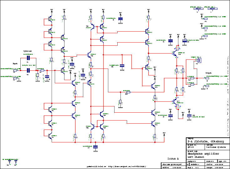
Click on the picture to get a larger view. The picture shows the schematics of the amp. Of course you can't use it for anything except for an overview. Please download the pdf-file instead if you want to see the details.
I have chosen to use current generators with cascodes as emitter loads. How much good the cascodes do is unknown at the moment. The only obvious disadvantage is a little bit reduced output voltage swing, otherwise only positive things, like less distotion and higher speed.
The current in the first stage (the input buffer) is set by T1, T3 and T2, T4 along with R4 and R5. I have transistors as diodes just to make it simpler when it comes to parts. The current is 0.65/560= 1,1 mA. The input stage of the amp is set by the relationship between R6/R10, and R7/R11, 10/2.2 = 4.5 => 5.3 mA. This current is then mirrored in the wilson current mirror, formed by T16, T18, T20, R8, R12 and T15, T17, T19, R9, R13. The resistors serves as local feedback which make the currents mirrors a little bit more linear.
The collectors of T19 and T20 creates a high impedance node and is also the output of the amp. This high impedance output must be buffered in order to useful. This is done with a diamond buffer. The current is given by the current in the mirror times R12/16 = 2.4 mA. The output stage runs in class A (which the whole amp does) 2.4 mA * R18/(R20//R22) = 10.2 mA.
My choice of currents is "average", because you both increase them and also decrease them. The max current is set by the max allowable power dissipation of the transistors. The small SOT23 types can take 310 mW or so and the SOT223, output transistors can dissipate 1.3 W but not in this application I imagine. More current mean slightly higher speed.
The input filter R2, C3 may be necessary if you are having trouble with RF interference. The values can be set to almost anything. The frequency is calculated by f= 1/(2*pi*R2*C3).
The pcb layout
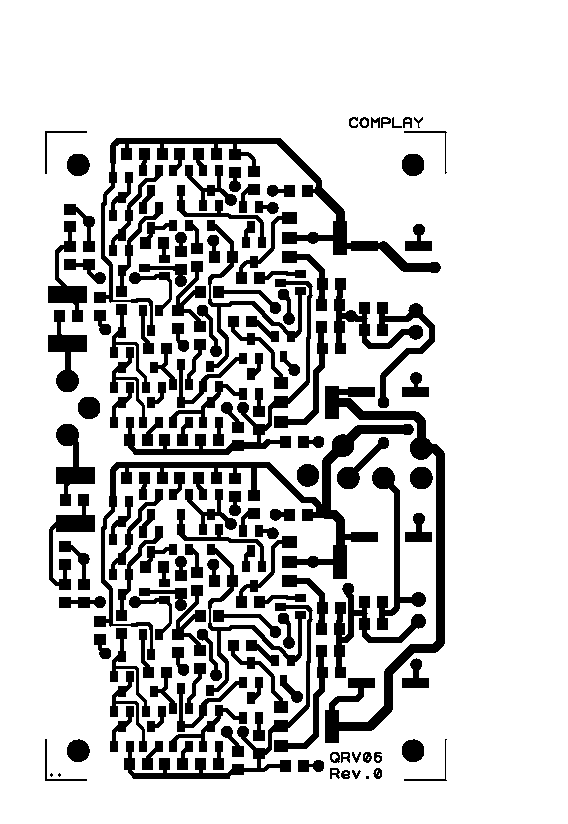
The component print
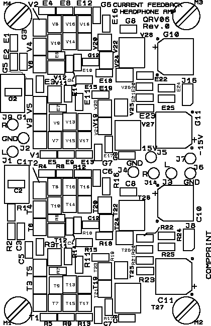
The picture shows the component print of the PCB. Of course you can't use it for anything except for an overview. Please download the pdf-file instead if you want to see the details.
The printed circuit board is made for one channel. It requires stabilized power supply. The pcb have groundplane on the lower (solder) side (not shown in pictures) which is essential in order to get good results. Almost everyone of the traces are on the solder side. The groundplane is very covering, only a few traces on the solder side.
The component side
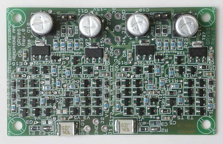
The picture shows the component side of the PCB. Of course you can't use it for anything except for an overview. Please download the pdf-file instead if you want to see the details.
Almost everyone of the traces are on the component side as you can see. The groundplane is on the solder side.
Build directions
This design is very easy to build. You should start with all low SMD parts. Solder in the electrolytic caps at last. For this solder job I recommend a good pair of tweezers. I use a type especially made for SMD. With this pair of tweezers I get a very good grip. You must also have a soldering iron with a small tip but.
If you don't want the input filter just short R2 with tin or a small wire.
Start with all low SMD parts
- Resistors
Transistors
Capacitors, not the electrolytic ones - Then continue with the high electrolytic caps
- Wires
Check the finished amp
Apply voltage and check the output voltage. Measure the DC voltage at the output. It should be the specified offset voltage, a couple of millivolts.
If the output offset voltage is a bit high you may need to adjust it.
Click on the pictures to get a larger view.
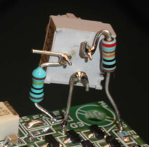
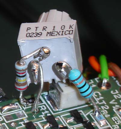
What you need for offset trim is a potentiometer and a resistor to inject current to the input. At the pictures you can see to different alternatives (choose one of them, the one at the right picture is the best). 10k pot + 100 k plus a 2.2 MOhms which you connect to the input. It depends if you shall connect the 100 k to plus or minus 15 volts. This is dependent of the sign if the base current of the input. Most likely you have more current gain in the NPN transistor, therefore the potentiometer must be connected to plus 15 volts.
Measure the quiescent current.
The whole amp is ready.
Good luck and happy listening.
Technical data
Click at the picture in order to get a larger view.
| Frequency response: | 0 Hz - 25 MHz(?), more than 10 MHz |
| Frequency response with input filter | 0 Hz - 1.29 MHz, -3 dB |
| Power bandwidth at 7 Vrms, 50 ohms: | 0 Hz - 25 MHz(?), more than 10 MHz |
| Equivalent input noise: | 0,6 µV |
| Signal to noise ratio: | 112 dB at 1 V out |
| Dynamic headroom: | 129 dB |
| Distortion: | 0,00046% |
| Slew rate: | 3000 V/us |
| Step response: | Perfect without overshoot |
| Gain: | 4 (12 dB) |
| Input impedance: | >1 Mohms, pullup, pulldown resistors not included. |
| Output impedance: | 2.5 ohms |
| Output current: | 1 A peak |
| Supply voltage: | +- 6 to 24 V DC with chosen transistors |
| Dimensions: | 47,6 (1,875") x 76,2 (3,0") mm |


