The pcb layout
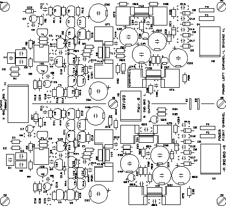
The component print
The picture shows the component print of the PCB. Of course you can't use it for anything except for an overview. Please download the pdf-file instead if you want to see the details.
The printed circuit board is made for two channels, contains everything, power supply and the amp itself except for connectors and transformer (or transformers). I have chosen not to have pcb mounted headphone and phono connectors because it's hard to fit in a case. My goal here is the use a 1 HE high case. You will need one or two transformers.
The pcb have groundplane on the upper side (not shown in pictures) which is essential in order to get good results.
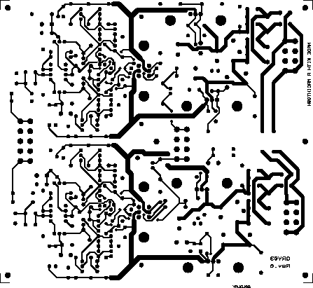
The solder side
The picture shows the solder side of the PCB. Of course you can't use it for anything except for an overview. Please download the pdf-file instead if you want to see the details.
Almost everyone of the traces are on the solder side. The groundplane is very covering, only a few traces on the component side, see below.
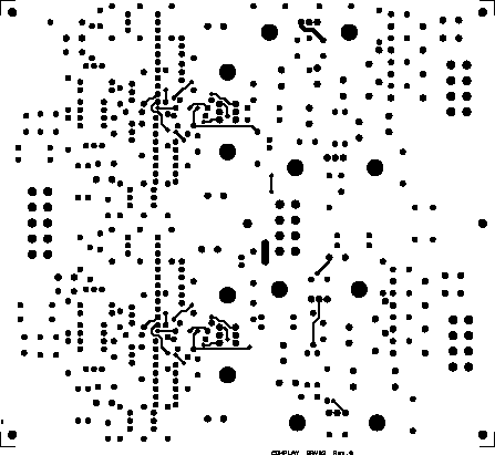
The component side
The picture shows the component side of the PCB. Of course you can't use it for anything except for an overview. Please download the pdf-file instead if you want to see the details.
Almost everyone of the traces are on the solder side as you can see. The groundplane is very covering, only a few traces on this side.
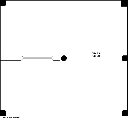
The groundplane mask
The picture shows the groundplane mask of the PCB. Of course you can't use it for anything except for an overview. Please download the pdf-file instead if you want to see the details.
The black area is without groundplane.
The hot relief pads
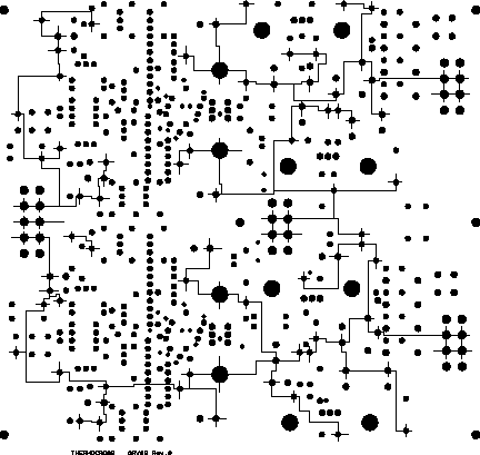
The picture shows the pads which are connected to groundplane of the PCB. Of course you can't use it for anything except for an overview. Please download the pdf-file instead if you want to see the details.
Each "cross" at the pads is a ground connection. This file is used together with the component side in a sandwich. I use this technique because my cad program has a very slow groundplane generation.

