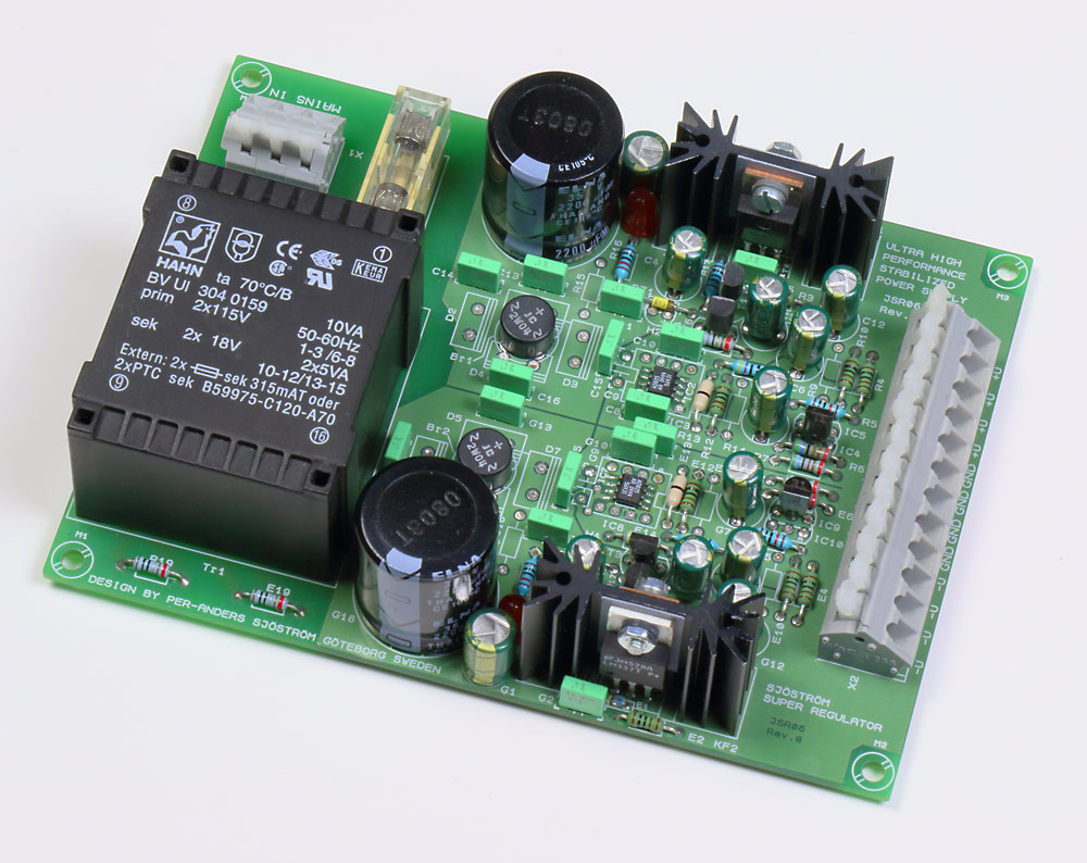
JSR-06 The Sjöström Super Regulator Power Supply
Click on the pictures to get a larger view.
Some background can be found in my JSR-01 project.
This design is based on my JSR-01 project and the goal was to make the pcb with hole mounted parts as small and versatile as possible.
The design
The design is based nearly to 100% of the original super regulator. My design goal here was to make a complete power supply, universal with many options and great flexibility.
This design has very interesting features:
- Extremely low output noise.
- Very low output impedance in the audioband.
- Easy to change the output voltage
- 115 or 230 VAC as input voltage
- Standard rectifier bridge or high performance built by discrete parts with sizes up to TO220, like MUR820, MUR860 or similar.
- Well-known and well-tested in serious and demanding applications.
- The pcb has room for holemounted DIL08 opamps or for surface mounted SO08 opamps.
- Snubberized raw voltage using 0805 SMD resistors. This is for removing resonance's.
- LM431 or LM385 as reference but I have made markings for anode, cathode and reference so it will be easy to mount any other 2- or 3 pin device like LM329.
- Extra trimming resistor for the LM431 voltage reference.
- Extra trimming resistors for tuning the output voltage.
- Frequency compensation for the opamp added as an option. By that you are more free of choosing opamp.
- Two methods of feeding the opamp with supply voltage.
- All resistors 10 mm between the holes so it is possible to use a cut and bending machine for those parts.
- Current peak limiting resistor after the rectifier bridges. Reduces the harmonics in the raw voltage.
- Not particularly hard to make to independent regulators. Convenient if you want to make two positive voltages. This is not tested and verified.
The schematics
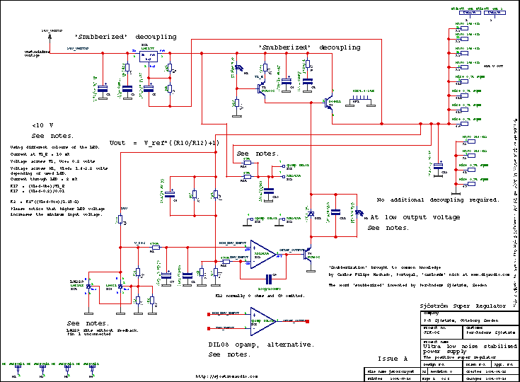
Click on the picture to get a larger view. The picture shows the schematics of the amp. Of course you can't use it for anything except for an overview. Please download the pdf-file instead if you want to see the details.
I recommend that you download the schematics and print it so you can follow the describing text more carefully.
Circuit description
Only the positive side is discussed. The same things apply for the negative side. The only thing which is not 100% alike is the connection of the reference because there is only one polarity of those.
The reference
As reference I have chosen to have maximum flexibility, therefore I have chosen LM431 which is easy obtainable. Virtual any reference will fit as long as the voltage is above the common mode limit for the used opamp. 2.5-7 V will work and in some cases also 1.2 V. At the moment I have tested 1.55 V from a red LED with perfect results. I have used LM431 and this very cheap reference is rather, no, very good, although not as nearly as good as LM329 but much, much better than a regular zener diode (which also can used). As a little help if you use some other reference I have written R(Ref), A(Anode) and C(Cathode) so you can connect almost any reference. R4 is carefully selected and may be changed if especially lower voltages are to be chosen. See instructions for this.
Notice that if you want to use some other reference like LM385 for instance you must read the datasheet carefully. LM385 can only withstand 5 volts max and the ADJ pin is different. At the moment only LM431 and LM329 are verified and work good.
The reference voltage is filtered by R8 and C7, C8 in order to remove the noise and as a side effect you will get a smooth startup. R8 should optimally be R10 and R12 in parallel but I consider this not extremely important. You can either choose 499 ohms or simply solder two 1 kohms on top of each other. If you have matched input impedance's you will minimize the input offset and also the drift with temperature (not very important in audio applications). It may also be good when it comes to common mode rejection. Since the whole design is placed on a groundplane I'll gather that high frequency problems are not so big so you must take this into account. R13 and C9 are parts for "just in case", to tailoring the frequency properties. Normally R13 is only a wire jumper and C9 is omitted. Times when you'll need this is when the output stage is much slower than now. If you'll have transistors with Ft of 5-10 MHz and a fast opamp like the used one. I'll guess the regulator won't get stable without slowering down the opamp. If you have D44H11 and D45H11 you can have a 30-50 MHz opamp like AD825 without any problems.
For low voltages it becomes rather complicated to calculate the resistor for the reference if it is a LM431 and similar with feedback. It's easy to get a hang-up at a voltage lower than the reference. The reason for this is that the feedback of the reference serves as a plain voltage divider so in order to get it working properly you must choose the resistors with taste. In the partslist there will be a couple of tested combinations with parts and output voltages.
The opamp
The opamp can be almost any type (DIL08 holemounted or SO08 surface mounted) as long it's not too fast, faster than the output stage. The maximum speed of the opamp at unity gain is around 30-40 MHz. The AD825 has the bandwidth of 34-37 MHz at unity gain. If extremely low noise is important AD797 might be suitable (although not very stable in some cases, avoid it if possible) but if "low" noise is sufficient I think any good audio opamp will do, like AD8610, OPA134 etc. Even good old NE5534 may work but I haven't tested this opamp. The only thing you must think of is the common mode limits for the inputs of the opamp. At startup it's important that the opamp has a predictable behavior, especially sensitive is this for a negative regulator.
At the moment only AD825 is tested for 5-15 volts, both positive and negative output voltages. I have had reports about OPA134 with results.
Power for the opamp
You can either take the power from the output or before the pass transistor T4(T5). What you choose is dependent of used opamp and how low the minimum supply voltage is (see the datasheet for this parameter). Minimum voltage for AD797 is 10 volts so if you want to be really sure you must feed it from the unregulated side if you want less than 10 volts out. Parts which are involved in this are R14 and R15.
AD825 has 6 volts as minimum but I have tested down to 3.1 volts with good results. This was valid for the tested regulator and the used AD825 but I'm not sure every AD825 will work.
Positive regulator, power from the output
R14 = used
R15 = not used
Positive regulator, power from the unregulated side
R14 = not used
R15 = used
The feedback network
The feedback network is very simple, only R10 and R12. R9 and R11 are for trimming the voltage if necessary. C6 reduces the output impedance half of it's the value. This capacitor is hardly necessary in real life but if you want lower output impedance you should use it. The values of the feedback resistors should be a low as possible considering the max power dissipation. It serves to purposes. The first is to create a voltage divider with good high frequency properties (avoiding unstability) and also to draw current out of the pass transistor, T4(T5). If current flows all the time also the output impedance can be kept low. It's also important for stability reasons.
The output voltage is determined by the reference voltage * (R10/R12 + 1)
The output stage
The output stage is rather unusual. Normally you have only one emitter follower, maybe together with a driver transistor forming a Darlington transistor. This type of output stage is rather slow. To speed things up the driver transistor is changed to a class A emitter follower as the driver for the pass transistor. The load of the emitter follower (T3/T6) is a current source formed by a reference voltage, the LED H1 (makes a nice glow) and R17 together with T1/T2. The current through the LED should be 1-3 mA. If you want very low voltages you must change the value of R16.
The driver is also a bit backwards. This creates a very special and also very important feature, the possibility to a safe power up of the opamp. The output stage deliver max output voltage when the opamp is inactive. This makes the opamp come alive at startup. The zener DZ1 increases the startup voltage and creates also a necessary DC shift so the output of the opamp works at ideally at half the output voltage. This zener voltage must be decreased when lower output voltages are wanted. For 5 volts it's sufficient with a diode or a red LED in the forward direction, creating only 0.7-1.6 volts. T5/T6 is added compared to Walt Jung's original (but Mr. Kaneda had it) and unloads the opamp from the drive currents. C11 takes down the impedance of the zener.
If you are interested in low voltages you must see to that the current through the LED H1 is sufficient. Strive to have as much current so you will see some light from the LED which is 0.5-2 mA. R13 is 10k for over 10 volts out but for low voltages you may decrease R13 to 1k.
Colour of the LED H1 and H3
You can use red, green and yellow LED's but avoid blue and white if you don't have plenty of raw voltage because blue and white will increase the minimum input voltage by 2-3 volts. This is rather unnecessary and causes only higher power losses but depending of application this may not be a problem.
No short circuit limiting
The regulator is a bit vulnerable against short circuit so I'll suggest you are careful when you are connecting the load. The LM317 has current limiting so you will have to trust this IC but this IC isn't indestructible according to my own experience. I recommend careful handling.
Choice of resistors
I recommend plain 0.6 W 1% metal film resistors as a good start. It's up to you to test other types.
The tolerance is not either very important but in case you wonder R10 and R12 in parallel should be close to the value of R8.
Choice of non-electrolytic caps
I recommend small polyester types but any good capacitor with good HF-properties will do. Even good ceramics will work. Tolerance is unimportant, only HF-properties are.
Choice of electrolytic caps
I recommend any type, from general purpose to low impedance types. I have used Sanyo MV-AX, low impedance with good results.
Tolerance is unimportant but check voltage rating.
Build directions
If you plan to use SOIC opamps you may start soldering them because if you not have a small soldering iron it may be hard to do it later. If you have a normal iron with a small tip it's not that hard to solder those IC's later.
- 0805 snubber resistors, 1 ohms or 0.5 ohms, two 1 ohms on top of each other. You can also put a tin drop or a wire there if you don't want this snubber.
- Wire jumper at B1 for 230 volts and B2, B3 for 115 volts. Place the jumper or jumpers on the solderside, otherwise hard to change if necessary. Cut the wires in the componentside which are under the transformer.
- All small low parts like resistors, zeners. Notice: zener OR LED, see the text above. Notice also the polarity of those parts.
- Opamps
- Plastic caps
- Small signal transistors, reference IC's
- LED's
- Rectifier bridges, or discrete power diodes
- Big electrolytic caps
- Fuse holder with insulation cover, see picture
- Varistor
- Connectors
- Heatsinks with regulators and power transistors. The heatsinks are grounded but none of the parts have their cases connected to ground. Therefore they must be insulated with a washer and bush. The washer may be made of Kapton (orange plastic), silicone rubber or mica. If silicone rubber is used there is no need for heat compound (white messy grease, increases the heat transfer). You don't need any grease either for mica or Kapton washers if the power dissipation is low, like 2-3 watts. In case of you'll use heat compound, apply a THIN layer on both sides of the washer. A thick layer grease will create a huge sticky mess, avoid it. Mount the parts first on the heatsink, then solder the parts and also the heatsink but it may be a good idea to solder the heatsink with only a small drop of tin, only to keep it in place. If you of some reason want to remove it it's easier if it isn't so thoroughly soldered.
Test
Connect 230 or 115 VAC. Observe the LED's H1 and H2 which should be lit. Measure the output voltage without any load. It should be stable within the last digit on your DVM. If you want to trim the voltage you could either do it changing the reference voltage or if you have a fixed reference you can use R9 and R11.
Connect a load for getting 100 mA output current. 150 ohms for 15 volts. The voltage should still be stable and change very little compared to the voltage when without any load.
Measure the voltage between the raw voltage and the output. Should be at least 5 volts if the LM317 is used and 2-3 volts if not. Suitable test point is D1, cathode, just above the "+" connection of the rectifier bridge Br1.
The PCB layout
The component print
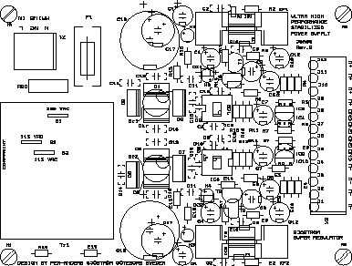
The picture shows the component print of the PCB. Of course you can't use it for anything except for an overview. Please download the pdf-file instead if you want to see the details.
The printed circuit board is made of 50 um thick copper and has a groundplane on the component side.
The component side
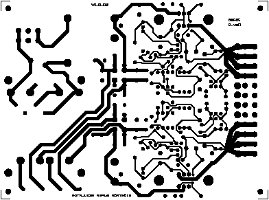
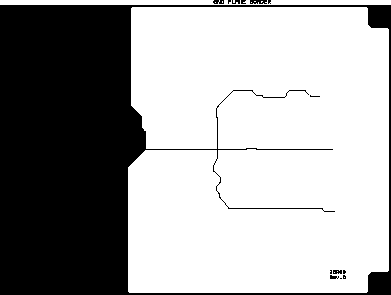
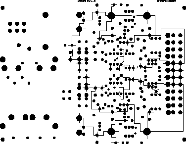
The picture shows from the left: the component side, the solder side, the groundplane mask (black areas are not groundplane) and last the thermo pads. of the PCB. Please download the pdf-file instead if you want to see the details.
Most of the traces are on the solder side.
Technical data
| Operating voltage: | 115 or 230 V AC, max 35 V DC in. |
| Output voltage: | 5-30 V |
| Hum and noise at full output current: | Down to 1 µV or below depending of component choices |
| Max current: | TBD Approx 1A at 15 volts and an external transformer and additional cooling. |
| Max continuous current: | TBD Approx 100 mA at 15 volts but more current at lower output voltages. Used transformer sets the limit. If external transformer is used with 2 x 18 VAC more current is possible. 200-300 mA is possible. |
| Dimensions: | 137 (5,4") x 102 (4") mm |

