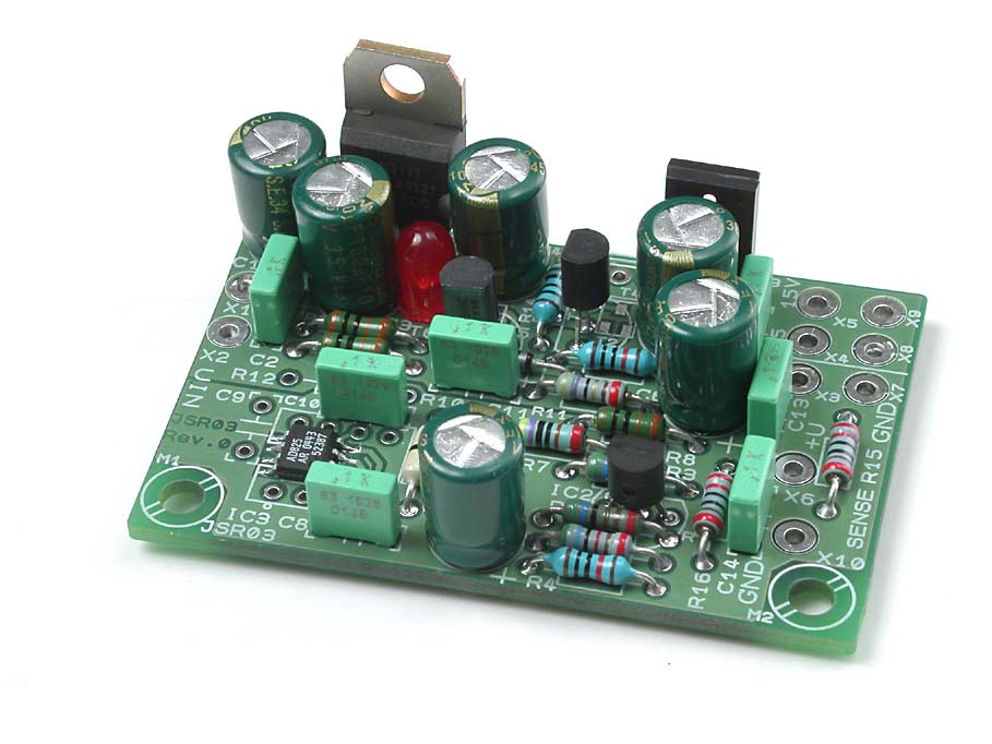
Page 6 of 7
The PCB layout
Click on the pictures to get a larger view.
The component print
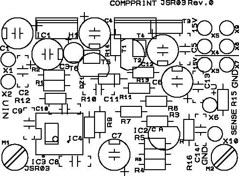
The picture shows the component print of the PCB. Of course you can't use it for anything except for an overview. Please download the pdf-file instead if you want to see the details.
The printed circuit board will be made of 50 um thick copper and has a groundplane on the solder side.
The component side
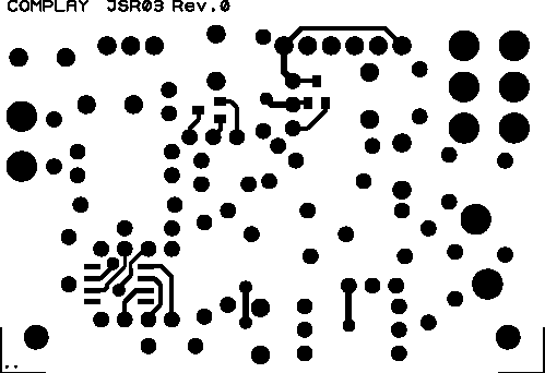
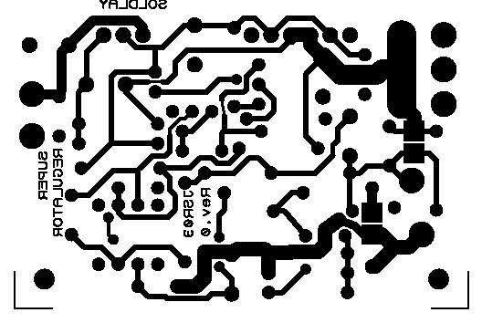
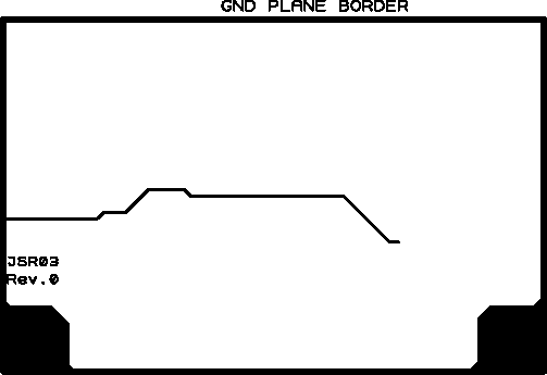
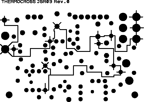
The picture shows from the left: the component side, the solder side, the groundplane mask (black areas are not groundplane) and last the thermo pads. of the PCB. Please download the pdf-file instead if you want to see the details.
Most of the traces are on the component side.
