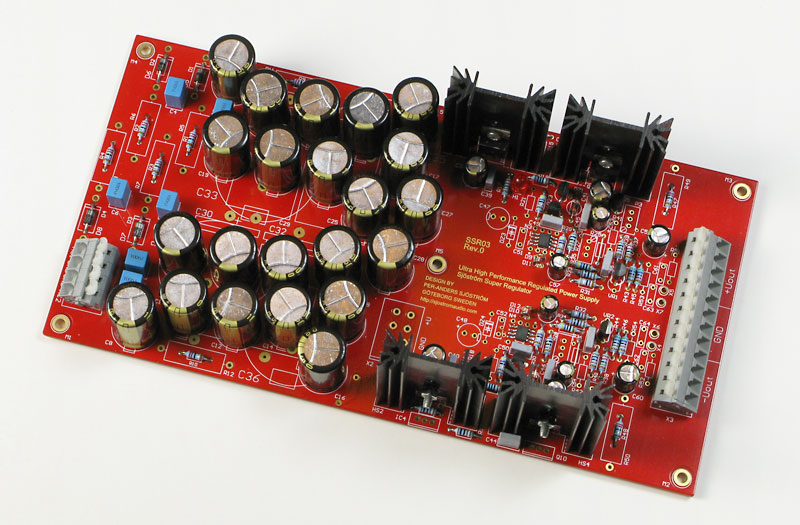
SSR-04 The Sjöström Super Regulator Power Supply

Click on the picture to get a larger view.
Some background can be found in my SSR-01 project.
This design is based on my SSR-01 project and the goal was to make the pcb with hole mounted parts as versatile as possible.
Interesting features
- 2-layer pcb with 70 um (2 oz.) copper.
- Gold pads.
- Extremely low noise.
- Extremely low output impedance in the audioband.
- Easy to change voltage
- Well-known and well-tested in serious and demanding applications.
- Option for DIL08 or SO08 opamp.
- LM431 (and similar) reference or devices like LM329. The pcb has an universal footprint.
- Trimming options for both the reference and the feedback. Room for extra resistors and trimpots.
- Option for using two different kinds of smoothing caps, radial or 10 mm snap-in.
- Output with sense inputs.
- All resistors 10 mm so it is possible to use a cut and bending machine for those parts.
Option for using higher voltage than the max supply voltage for the opamp.
The background
This design is based on my SSR-01 project so please go there and read about the super regulator details.
The basic idea is old as you can see and here I have taken two regulator circuits and a rectifier section to form a complete ultra stable power supply with extremely low noise out.The regulator from 1961
The basic idea has been around for at least 52 years.
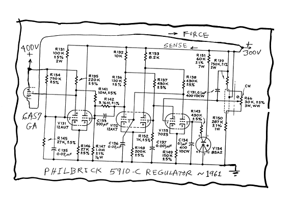
Bob Pease has dug up some info about the Philbrick tube super regulator . The circuit solution can be traced back to 1961 at least. Change all triodes to transistors and you'll see that this is really a super regulator.
The regulator from 1977
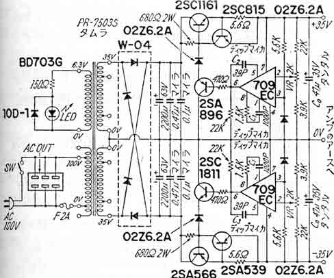
The Super Regulator from 1977, design by Mr. Kaneda.
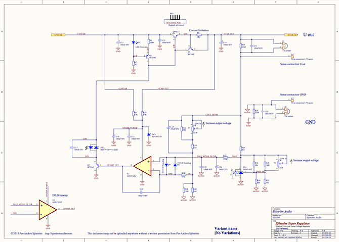
The design
Below you can see the schematics.
The schematics
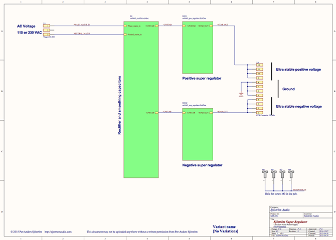
Click on the picture to get a larger view.
First page is showing the block diagram. First block is the transformer and the rectifiers with smoothing capicators. The two other blocks are the super regulator circuits, one for the positive output voltage and the other one for the negative.
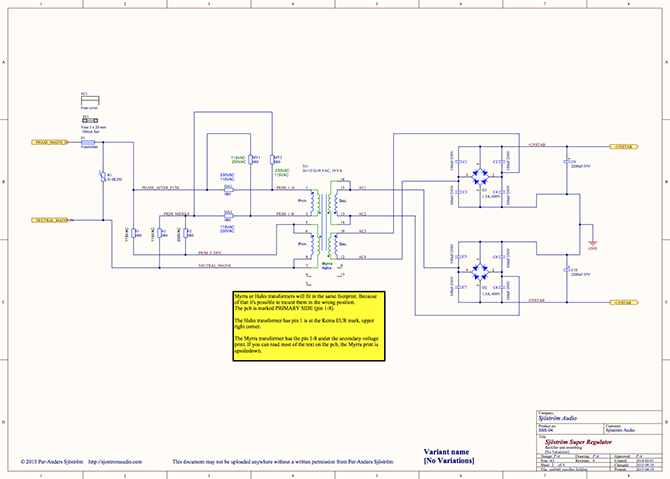
Click on the picture to get a larger view.
Second page is showing the transformer, the rectifier and the smoothing section. You have two options for capacitor choice, radial types or snap-in types. The transformer footprint is adopted for two types of pinout, one fitting Hahn transformers and one for Myrra. This footprint removes the possibility not mounting the transformer in the right way. See more about this in the circuit description.
Click on the picture to get a larger view.
Third (and fourth, not shown here) page is showing the super regulator, the heart of the design.
I recommend that you download the schematics and print it so you can follow the describing text more carefully.
Circuit description
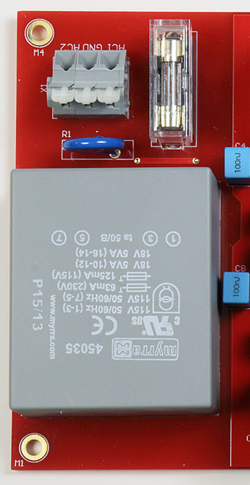
The transformer
The pcb has an universal footprint so two types of transformer pinning layout can be used. The brand Hahn (black transformers) and Myrra (grey transformers) can be used. The performance between the brands seems to be equal. The power rating is 10 VA.
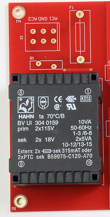
Picture of the mounting position of Hahn and Myrra transformers. Click on the pictures to get a larger view.
Notice that the two brands of transformers are positioned. The printed text should be upsideown for the Myrra type. Se more details in the build section
The rectifier
The design use a full-wave rectifier bridge rated to 1 ampere. A capacitor is placed across each diode in order to reduce switching noise.
The pcb has room for 10 mm snap-in caps or radial caps.
The reference (positive side)
As reference I have chosen to have maximum flexibility. Virtual any reference (VR1) will fit as long as the voltage is above the common mode limit for the used opamp. 2.5-7 V will work and in some cases also down to 1.2 V. LM431 and LM329 is supported. Other references will work but check the pinout first. The LM431 (thick outline in the silkscreen print) has four resistors R26, R28, R30, R32 and a trimpotentiometer P3 in order to trim the reference voltage. You can't trim the LM329.
The reference voltage is filtered by R22 and C27, C29 in order to remove the noise and as a side effect you will get a smooth startup. R35 should optimally be the value of the feedback network impedance, (R14+R16)//R18//R20. //= means in parallel.
If you have 1k+1k in the feedback you can for the R22 either choose 499 ohms or simply solder two 1 kohms on top of each other. If you have matched input impedance's you will minimize the input offset and also the drift with temperature (not very important in audio applications). It may also be good when it comes to common mode rejection. Since the whole design is placed on a groundplane I gather that high frequency problems are not so big so you must take this into account. R12 and C23 are parts for "just in case", to customize the frequency properties. Normally R12 is only a wire jumper or a low value resistor and C23 is omitted.
The opamp (positive side)
The opamp (N1) can be almost any type as long it's not too fast, faster than the output stage. The maximum speed of the opamp at unity gain is around 30-40 MHz. The AD825 has the bandwidth of 34-37 MHz at unity gain and the AD797 has unity gain bandwidth of approx. 30 MHz. If extremely low noise is important AD797, LT1012 and LT1115 might be suitable but if "low" noise is sufficient I think any good audio opamp will do, like AD8610, OPA134 etc. Even good old NE5534 may work but I haven't tested this opamp. The only thing you must think of is the common mode limits for the inputs of the opamp. At start-up it's important that the opamp has predictable behaviour, especially sensitive is this for a negative regulator.
At the moment only AD797 and AD825 are tested for 5-24 volts, both positive and negative output voltages. Others have tested LT1028/LT1115 with good results.
Input protection of the opamp (positive side)
D9 and D11 is input protection fo the opamp in case you can get differential voltages higher than the maximum ratings, for instance at short circuit conditions. Under controlled conditions you can omit these diodes since they introduce an extra capacitance at the input.
Power for the opamp (positive side)
You can either take the power from the output or before the pass transistor Q3. What you choose is dependent of used opamp and how low the minimum supply voltage is (see the datasheet of the opamp for this parameter). Minimum voltage for AD797 is 10 volts so if you want to be really sure you must feed it from the unregulated side if you want less than 10 volts out. Parts which are involved in this are R8-R10 and C19, C21. The DZ3 must be used if the supply voltage is more than the maxium supply voltage of used opamp. The value of the zener should be lower than the maximum supply voltage of the opamp.
The feedback network (positive side)
The feedback network is R14+R16 as the upper part. R14 is normally a wire and is used for trimming purposes. R18 in parallel of R20 is the lower part of the feedback and R18 is for trimming also. P1 can also be used if you want a variable output voltage, recommended if you use a fixed voltage reference like the LM329.
C25 reduces the gain and by this increase of the feedback which also reduces the output impedance. This capacitor is hardly necessary in real life (if the gain is 2) but if you want lower output impedance you should use it. The values of the feedback resistors should be a low as possible considering the max power dissipation. It serves two purposes. The first is to create a voltage divider with good high frequency properties (avoiding unstability) and also to draw current out of the pass transistor, Q3. If current flows all the time the output impedance can be kept low. It's also important for stability reasons.
The output voltage is determined by
Vout = Vref*(((R14//P1)+R16)/(R18//R20)+1)
The output stage (positive side)
The output stage is rather unusual. Normally you have only one emitter follower, maybe together with a driver transistor forming a Darlington transistor. This type of output stage is rather slow. To speed things up the driver transistor (Q1) is changed to a class A emitter follower as the driver for the pass transistor (Q3). The load of the emitter follower (Q1) is a current source formed by a reference voltage, the LED H1 (makes a nice glow) and R2 together with Q1. The current through the LED should be 1-3 mA. If you want very low voltages you must change the value of R2. A side effect of the LED H1 is that you will get an indication when you have enough input voltage and you have a stable output voltage.
The driver is also a bit backwards. This creates a very special and also very important feature, the possibility to a safe power up of the opamp. The output stage deliver max output voltage when the opamp is inactive. This makes the opamp come alive. The zener DZ1 increases the startup voltage and creates also a necessary DC shift so the output of the opamp works at ideally at half the output voltage. This zener voltage must be decreased when lower output voltages are wanted. For 5 volts it's sufficient with a LED in the forward direction, creating only 1.6 volts. Q7 is added compared to Walt Jung's original (but Mr. Kaneda had it) and unloads the opamp from the drive currents. C17 takes down the impedance of the zener.
No (or limited) current limiting .... or have it (positive side)
I have increased the current of the driver Q1 for higher speed but this makes also the regulator more vulnerable against short circuit so I suggest you are careful when you are connecting and not are using the current limiter, Q5. It is possible to destroy the regulator the regulator if the current limiter is omitted. Adding short circuit protection will increase the output impedance if you not implement an advanced circuit which requires lot's of pcb space. The current limit is set to 0.65/R47. If you want to omit the current limitation, inser a wire between Q5, collector (pin 1) and emitter (pin 3) and a wire at R6.
Capacitive load and C15 (positive side)
The faster opamps you have, the more sensitive against capacitive load the regulator will get, meaning low loss capacitive load. The regulator has a minimum load of 0.3-0.5 ohms and if you have a 100 nF connected very close to the output transistor you can get an impedance lower than 0.5 ohms. This frequency will be at 3 MHz. Therefore the C15 must not be too "good". In fact a "normal" cap is sufficient and if you choose a low impedance cap you may experience unstability. If you use a fast opamp, it simulates a cap rather high up in frequency so serious decoupling this close to the output transistor isn't necessary but if you only have 30 mm wire the regulator can take 100 nF or more. The short wire creates a small inductance that is sufficient in order to limit the lowest impedance.
The "sense" connections (positive side)
The sense connections are a bit overkill but if anyone wants these I have added this feature. The sense function is mainly to subtract or eliminate the losses in the power wires, which won't be especially large. It's just milliamps. If you want this feature make sure that the sense wires are close to the power wires so instability can be avoided. If you don't want to use this feature, just put two tin jumpers on the pcb solder side, marked J1 and J2. If you are sure that you never will use the sense function you can also omit R34, R36, C31 and C33.
The pcb layout
Click on the picture to get a larger view.
Please download the pdf of the pcb layout for more info.
The pcb is made of 70 um (2 oz.) copper and has two layers. There are groundplanes on both sides and also a special groundplane for the signal ground.
In several places there are room for alternative parts such as regulators and transistors for external heatsinks, DIL08 opamp (N2) and voltage references VR1. Thin outline is for LM329 and bold outline LM431 and other pin compatible parts.
My design SSR01 (similar to this) is in the top of super regulators in the market and one of the best in "jackinnj"'s test in Linear Audio's big regulator test. It's worth noticing that not every regulator had the super regulator topology.
Assembly instructions
This design is very easy to build. . You can solder the parts in the order you'll like but it may be practical to start with all low (height over the pcb) parts such as resistors and then take higher parts.
Start with all low parts except for the output power amp and the opamp.
- Opamp if it's a SMD type. It's hard to solder if you have any parts around the opamp.
- Resistors, jumpers, also at the transformer. See instructions below how to set the primary voltage 230 or 115 VAC.
- Zener diodes
- Diodes. Notice that the diodes, D9-D12, near the opamps are mounted in a special way, see the photo. They are standing up. Be careful when you bend of of the legs.
- Rectifier bridge. Don't cut the AC wires of the rectifiers in case you want to the each regulator with an external lab power supply.
- Plastic capacitors
- Transistors, voltage reference. Fat outline = LM431. Thin outline = LM329 or other 2-pin devices.
- LED
- Trim pot (if you use it)
- Fuse holder
- Varistor
- Capacitors, elelctrolytic
- Power transistor. Mount them first in the heatsink, then solder them. You won't need any insulation between the semiconductor and the heatsink but heat compund may be used to increase the heat transfer. Pay also attention to that the heatsink isn't in touch with the groundplane. Solder the heatsink into the pcb when you see that everything is working.
- Connectors
- Transformer. Wait with this until the regulators are tested. ATTENTION about the mounting direction, see details below
Besides from these instructions the regulator is pretty easy to build but pay attention how you should mount all polarized parts. See pictures below and also the pdf file. In the pdf file I have made placement pictures with extra clear markings for each part. Print it and have it beside you when you solder.
The Hahn transformer
230 VAC
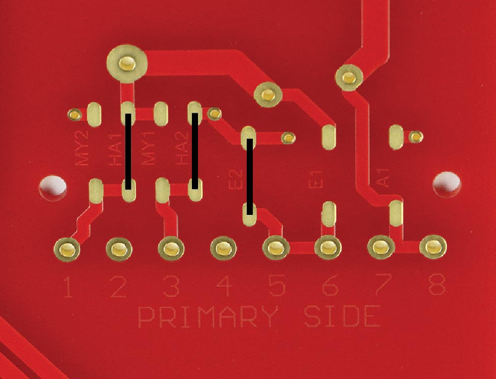
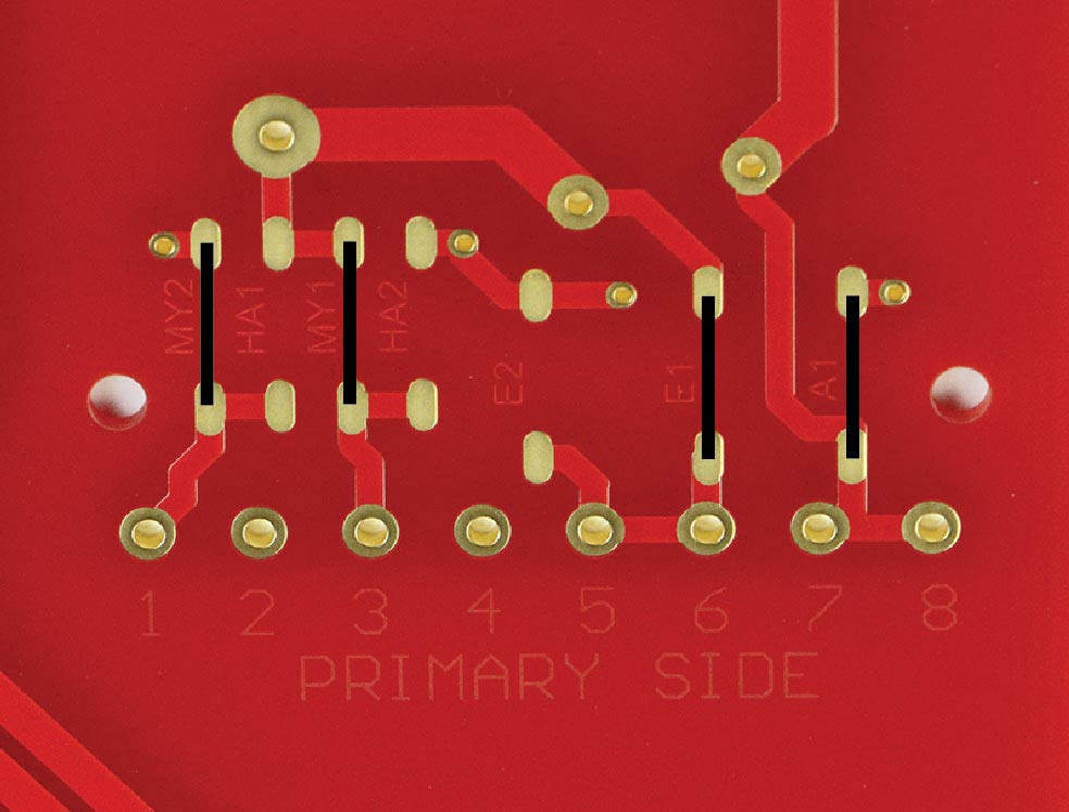
Hahn transformer, 230 VAC. Click on the picture to get a larger view.
In the soldermask you can see if you look closely, HA1 and HA2 (HA=Hahn). Put a wire in those positions. E2 is used for 230 VAC.
115 VAC
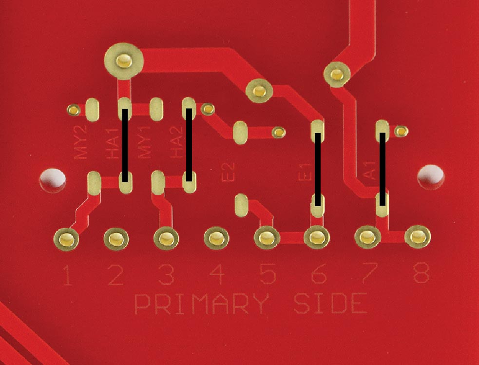
Hahn transformer, 115 VAC. Click on the picture to get a larger view.
HA1 and HA2 (HA=Hahn). Put a wire in those positions. E1 and A1 are used for 115 VAC.
The Myrra transformer
230 VAC
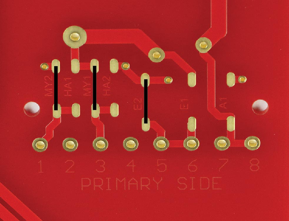
Myrra transformer, 230 VAC. Click on the picture to get a larger view.
MY1 and MY2 (MY=Myrra). Put a wire in those positions. E2 is used for 230 VAC.
115 VAC
Myrra transformer, 115 VAC. Click on the picture to get a larger view.
MY1 and MY2 (MY=Myrra). Put a wire in those positions. E1 and A1 are used for 115 VAC.
Detail of the positive half

Click on the picture to get a larger view.
Parts for ± 15 volts out using LM431 and a Myrra transformer.
Test
If you don't plan to use the "sense" function, put a tin blob on the solder side at J1, J2, J3 and J4 (see the schematics also).
- Use a regulated power supply and set the current limit to 50-100 mA or something low.
- Connect the external power supply at the uncut wires of the rectifier. (test one half at the time)
- Connect a voltmeter at the output.
- Turn up the voltage slowly and observe the output and the current consumption. When the LED H1 starts to shine you should have a stable output voltage.
- Add a load to check is the voltage still is stable including some warm-up of the opamp and the voltage reference (a few millivolts).
- Do the same thing for the negative side.
- Solder the transformer and pay attention to the jumpers, HA1, HA2, MY1, M2, E1, E2 and A1.
- Connect the mains voltage and observe a stable output voltage.
Technical data
| Operating voltage: | Max 50 V, less current at high voltage in. Min 3 volts more than output voltage. |
| Output voltage: | 5-40 V, down to 3 volts is possible. |
| Hum and noise at full output current: | Down to 0.9 µV or below depending of component choices |
| Max current: | Approx. 1 A peak |
| Max continuous current: | Approx. 1 A depending of ambient temperature and mounting (cooling). |
| Dimensions: | 226 (8.9") x 114 (4.51") mm |
Measurements are done by John Walton, jackinj, with an Audio Precision measurement system.
| Used parts | LM329, AD825 | LM329, AD797 | LM329, LT1028 |
| No filter: | 15.14 µV | 5.67 µV | 6.95 µV |
| A-Weighted: | 2.38 µV | 1.03 µV | 1.00 µV |
| CCIR-486: | 6.40 µV | 2.04 µV | 2.02 µV |
| CCIR-2K(Avg): | 3.03 µV | 0.941 µV | 0.921 µV |
| 22-22K: | 3.52 uV | 2.37 uV | 1.70 uV |
