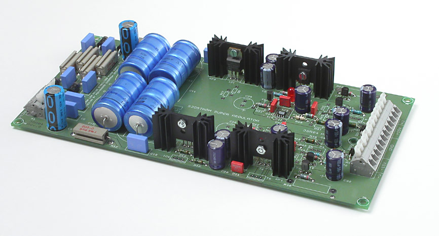
Circuit description
The reference
The chosen reference here is the common and rather good LM431. It gives a reference voltage from 2.5 volts and up. The value is determined by R43 and R45 according to the formula:
Vref_out = Vref x R43/R45 + 1
Normally you should have half the output volatge as reference voltage. 15 volts out gives you 7.5 volts as reference voltage. The reason why is that gain of 2 is preferable.
Lot's of other voltage references could be chosen, anything from a plain zener diode, a LED over to advanced zeners like LM329 and the even more advanced LM399 or LM3999! LM329 is a very good choice if you want a very good reference with very low noise and not so high price. LM329 was also Mr Walt Jung's favourite choice but LM431 is much easier to get and frankly quite good.
The opamp
The opamp can be almost any type (DIL08 holemounted or SO08 surface mounted) as long it's not too fast, faster than the output stage. The maximum speed of the opamp at unity gain is around 30-40 MHz. The AD825 has the bandwidth of 34-37 MHz at unity gain and the AD797 has unity gain bandwidth of approx. 30 MHz. If extremely low noise is important AD797 might be suitable but if "low" noise is sufficient I think any good audio opamp will do, like AD8610, OPA134 etc. Even good old NE5534 may work but I haven't tested this opamp. The only thing you must think of is the common mode limits for the inputs of the opamp. At start-up it's important that the opamp has a predictable behaviour, especially sensitive is this for a negative regulator.
At the moment only AD797 and AD825 are tested for 5-24 volts.
Power for the opamp
You can either take the power from the output or before the pass transistor T3 (T5). What you choose is dependent of used opamp and how low the minimum supply voltage is (see the datasheet for this parameter). Minimum voltage for AD797 is 10 volts so if you want to be really sure you must feed it from the unregulated side if you want less than 10 volts out. Parts which are involved in this are R19 and R21.
AD825 has 6 volts as minimum but I have tested down to 3.1 volts with good results. This was valid for the tested regulator and the used AD825 but I'm not sure every AD825 will work.
The feedback network
The feedback network is very simple, only R33 and R39 in it's simpliest way. R37, R35 and P1 are parts for trimming. C29 reduces the output impedance half of it's the value. This capacitor is hardly necessary in real life but if you want lower output impedance you should use it. The values of the feedback resistors should be a low as possible considering the max power dissipation. It serves to purposes. The first is to create a voltage divider with good high frequency properties (avoiding unstability) and also to draw current out of the pass transistor, T3 (T5). If current flows all the time also the output impedance can be kept low. It's also important for stability reasons.
The output voltage is determined by the reference voltage * (R33/R39 + 1)
The output stage
The output stage is rather unusual. Normally you have only one emitter follower, maybe together with a driver transistor forming a Darlington transistor. This type of output stage is rather slow, too slow here. To speed up things the driver transistor is changed to a class A emitter follower as the driver for the pass transistor. The load of the emitter follower (T5/T6) is a current source formed by a reference voltage, the LED H1 (makes a nice glow) and R13 together with T1/T2. The current through the LED should be 1-3 mA. If you want very low voltages you must change the value of R13.
The current through T1 is set to 10 mA and this is determined by R23 and used reference voltage, used LED. This current times the current gain of the output transistor T3(T5) will set the limit of possible output current which is 600 mA to over 1 A.
The current through T1 can be set lower and the max is set by max power dissipation of T1 and T9. Up to 25-30 mA is "normal" I think.
Worth noticing is also that using two silicone diodes (=1.3-1.4 V) will decrease possible losses and use of nicer colours than red, especially blue and white will increase the minimum input voltage and also increase losses in the T3 (T5). In the schematic you have formulas for calculating for different colours of the LED. You can't simply change the LED I'm afraid.
The driver is also a bit backwards. This creates a very special and also very important feature, the possibility to a safe power up of the opamp. The output stage deliver max output voltage when the opamp is inactive. This makes the opamp come alive. The zener DZ1 increases the startup voltage and creates also a necessary DC shift so the output of the opamp works at ideally at half the output voltage. This zener voltage must be decreased when lower output voltages are wanted. For 5 volts it's sufficient with a diode in the forward direction, creating only 0.7 volts. T9 is added compared to Walt Jung's original (but Mr. Kaneda had it) and unloads the opamp from the drive currents. C39 takes down the impedance of the zener.
If you are interested in low voltages you must see to that the current through the LED H1 is sufficient. Strive to have as much current so you will see some light from the LED which is 0.5-2 mA. R23 is 10k for over 10 volts out but for low voltages you may decrease R23 down to 1k.
For low voltages you must also change the DZ1. The value of this zener should be half of the output voltage. 5 volts out requires 1.6 volt at least which is a LED in forward direction.
Short circuit limiting
I have increased the current of the driver T1, for higher speed but this makes also the regulator more vulnerable against short circuit so I suggest you are careful when you are connecting. The LM317 has current limiting so you will have to trust this IC. I recommend careful handling though.
A real current limiting can be added by changing the wire in the R27 position to a resistor. T7 must also be mounted. The drawback is a bit increased output impedance.
Capacitive load
The faster opamps you have, the more sensitive against capacitive load the regulator will get, meaning low loss capacitive load. The regulator has a minimum load of 0.3-0.5 ohms and if you have a 100 nF connected very close to the output transistor you can get an impedance lower than 0.5 ohms. This frequency will be at 3 MHz. Therefore the C31 must not be too "good". In fact a "normal" cap is sufficient and if you choose a low impedance cap you may experience unstability. If you use a fast opamp, it simulates a cap rather high up in frequency so serious decoupling this close to the output transistor isn't necessary but if you only have 30 mm wire the regulator can take 100 nF or more. The short wire creates a small inductance which is sufficient in order to limit the lowest impedance.
