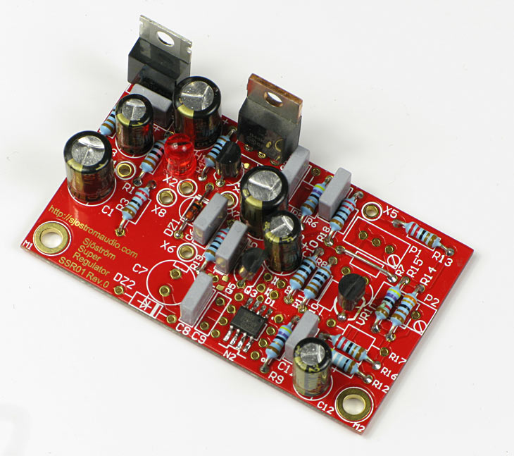
The pcb layout
Click on the picture to get a larger view.
Please download the pdf of the pcb layout for more info.
The pcb is made of 70 um (2 oz.) copper and all traces which will carry high currents are doubled. They are on both sides and the nets involved (see the schematics) are Uin, Pre_reg_out and Uout. The pcb consists of four layers (which is unique!) and the two inner layers are dedicated for power ground and signal ground. The advantage is that the pcb can have two whole ground planes without any traces. The signal ground is very sensistive and is the key to the very good performance of this compact pcb. The other two layers have traces and power ground but the ground planes are on those layers a bit more divided.
In several places there are room for alternative parts such as SOT23 transistors (Q4, Q5), DIL08 opamp (N2) and voltage references VR1. Thin outline is for LM329 and bold outline LM431 and other pin compatible parts.
My design is in the top of super regulators in the market and one of the best in "jackinnj"'s test in Linear Audio's big regulator test. It's worth noticing that not every regulator had the super regulator topology.


