QSX Mark III - The extreme phono (RIAA) amplifier
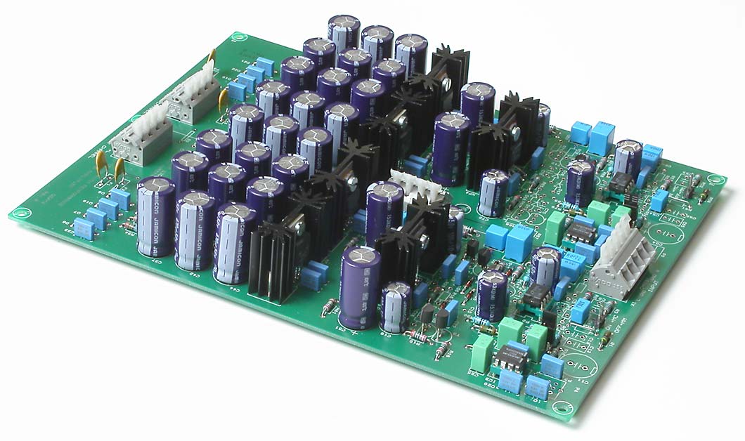
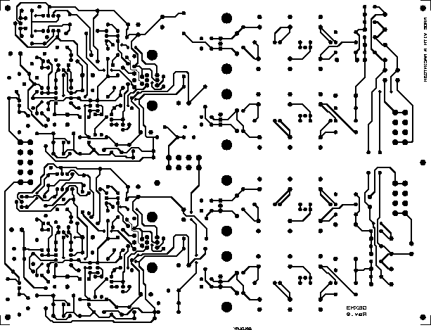
Click on the picture to get a larger view. The printed circuit board of the QSX Mark III Amplifier.
Interesting features
In order to get an extremely linear and extremely low distortion design I have taken a couple of measures:
- No capacitors in the signal paths
- Totally DC-coupled together with DC-servo
- The opamp is biased into class A with a JFET or bipolar transistor.
- Many decoupling capacitors and EMI-filters
- Powerful output buffer, intergrated or discrete, your choice.
- Power supply on the board, just add AC voltage.
- Professional quality printed circuit board with groundplane.
- The pcb has lot's of possibilities when it comes to tweaking.
The schematic
The schematic, page 1 and 3 of 3, the pre amplifier
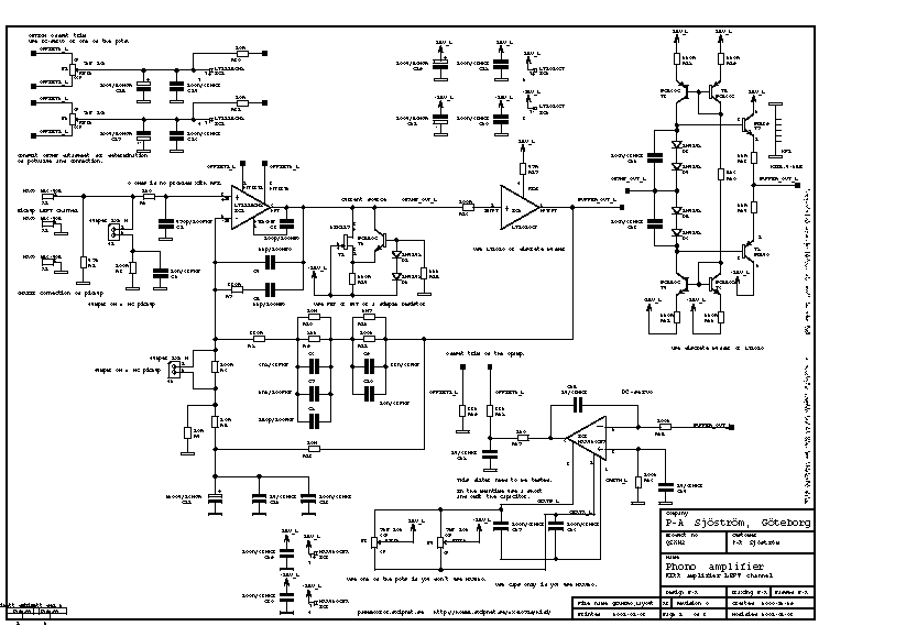
The picture shows page 1 and 3 of the schematic. Of course you can't use it for anything except for an overview. Please download the pdf-file instead if you want to see the details.
If you want a general description of the design, see the text down below.
The schematic, page 2 of 3, the power supply
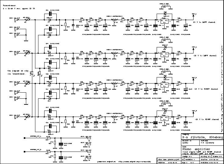
The picture shows page 2 and 4 of the schematic. Of course you can't use it for anything except for an overview. Please download the pdf-file instead if you want to see the details.
Circuit description
Please download all the schematic pages and print them out. It's much easier to understand what I'm talking about if you look at the circuits at the same time. I will only talk about the left channel. The two channels are identical.
The amp consist of a couple of blocks
- Opamp, extremely low noise och low distortion
- Crossover distortion reducer with a JFET or a BJT or a simple resistor
- Integrated buffer or discrete buffer with power transistors
- Feedback network, RIAA-network, with option for Linear Tech original (see picture below) and my own
- DC-servo with chopper stabilized opamp (ordinary precision type opamp can be used also)
- Offset adjusting pots (if you don't use DC-servo)
- Stabilized power supply, except for transformer (or transformers)
The main idea
The main design idea is taken from the datasheet of LT1115 which is an excellent opamp with extremely low noise, one of the lowest in the market despite the fact that the chip is nearly a decade old.
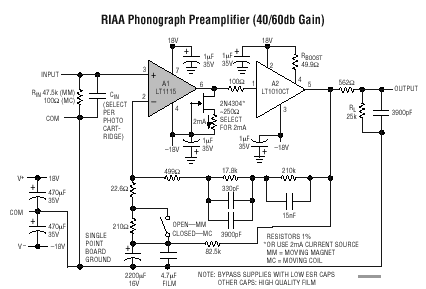
The picture above shows the original circuit which I think is rather well-done but nevertheless a few enhancements can be done.
The pcb is designed so you can build an exact copy of the original, therefore the RIAA network may seem a little bit odd in my design but if you take a closer look there are two different networks. The main thing I personally don't like is the 2200µF capacitors for DC-removal. I use a DC-servo instead. I have also trimmed the RIAA network in order to be even more accurate.
The picture shows the RIAA curve of the original design. Download the datasheet of LT1115 if you want a clearer picture.
RIAA-amp amplifies the signal and correct it according to the international RIAA-curve.
The capacitors for the RIAA-network should be high performing and with tolerance of less than 5%, preferable 2.5%. If you can't get hold of precision caps it's OK to measure up 5 or 10% caps. I think both polycarbonate and polyester will work rather well but I recommend polypropulene.
I you want any help measuring caps I can do that for you. I have a 0.25% LCR bridge. If you buy something from me you will get this for free otherwise I'll do it for 2 x postage.
No capacitors in the signal paths - DC-servo
A DC-servo eliminates the input offset, which always are present. No capacitors are the signal path. Therefore the offset voltage is about 1000 (MM mode) to 10000 (MC mode) times higher than in a normal AC-coupled amp. The residual offset comes from the DC-servo itself. The offset voltage is the DC-voltage at the output when you have no signal applied to the input. It comes from deficiencies in the input stage of the opamp.
LT1115 together with C11-C13 gives you excellent DC performance but if you like me don't like these caps you must use a DC-servo. It's virtually impossible to get good DC-performance without some kind of servo (based on good opamps).
The DC correction circuit here is kind of special. You can't use this approach to any opamp. You can use similar approach for other opamps but this is nothing for a newbeginner. It takes deep knowledge of the opamp and what's inside. Using the "Trial and error" method is doomed to fail. My method here is to manipulate with the offset trim inputs. These pins are directly connected to the input stage of the opamp. The alone resistor R29 together with R28 creates a basic balance. When R28 is raised from ground or lowered from ground you will get a small change in the balance of the input stage.
DC is sensed at the output and then integrated in the chopper stabilized opamp which creates an error voltage fed back into the main opamp.
How does the DC-servo work in detail?
The servo has some difficulties to be connected conventionally to the junction of the inverting input because of the low resistor values. The servo will consume a great deal of power but otherwise it's not a problem. My solution to manipulate with the offset adjusting inputs works only for LT1028/LT1115. It may work for other opamps but most likely the connection must be done with different resistor values and/or circuits. This is nothing for a newbeginner. It requires a great deal of knowledge in order to succeed.
Through R28 a small current is either injected or drained. C28 makes sure that no audio signal goes into the servo and also that the servo not introduces any noise.
You can choose from four options:
- Chopper stabilized operational amplifier with external auto-zero caps, MAX420, R25-R29, R74-R78, C24-C30, C77-C83, IC3 and IC8.
- Chopper stabilized operational amplifier with internal auto-zero caps, MAX430, R25-R29, R74-R78, C24, C25, C28-C30, C77, C78, C81-C83, IC3 and IC8.
- Conventional precision operational amplifier, R25-R29, R74-R78, C24, C25, C28-C30, C77, C78, C81-C83, IC3 and IC8 (OP07 or similar), P3, P7 or P4, P8, depening on chosen opamp.
- Plain trim potentiometers, P1, P5 or P2, P6, depening on chosen opamp.
All opamp choicies are good but they are listed in performance order. I don't recommend trim potentiometers but I have made room for them anyway. Chopper stabilized DC-servo is a nice overkill. Never seen before in a RIAA amp! Prove me wrong! Still if you want the job to be done with some technical sanity, use a opamp, a decent type with good DC-performance, slow and with low noise. The speed of the opamp should be not more than 1 V/µs. OP07 is a typical example of what you need.
The output stage
I have made options for two different kinds of output stages, one regular bipolar one with fast small power transistors and one integrated with the buffer LT1010. With this two choices I have made the design a little bit more "timeless". If you easily can get the LT1010, use it! My recommendation.
The bipolar (BJT) output stage
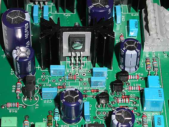
Click on the picture to get a larger view.
The monolithic (LT1010) output stage
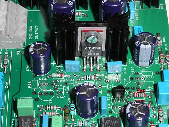
Click on the picture to get a larger view.
The Class A circuit
You can choose from three options:
- JFET, current source, T1, T9, R14 and R63. The value of these resistors need probably adjustment, higher value, 500 ohms or higher.
- BJT, current source, T2, T10, R14, R15, R63, R64, D1, D2, D13, D14
- Plain resistor, R14, R63 connected directly to the output. Suitable value 6.8-10 kohms.
The class A circuit can be omitted but it makes most benefit when the load from the opamp is small like when you use the LT1010 buffer. This circuit is very popular in the internet DIY community, never seen though in real life, in commercial products. It's cheap, easy to implement, doesn't do any harm for sure, can do good, not always the case. No harm in testing! Even a serious firm, Linear Technology suggests it.
Feedback
I have made room for additional feedback networks. This is only necessary if you have difficult loads. C3, C50, R7, R56, C5, C58. You may be forced to use them if you use the amp in some other application.
The input filter
It's very important to tune the input impedance in order to achieve flat frequency response. R1 together with R50 creates 47 kohms needed for most MM pickups and R3, R52 is for MC pickups.
R2, R51 together with C2, C54 is an EMI-filter. In order to achieve the lowest noise possible R2, R52 should be 0 ohm if you don't have any RF interference. If you have some trouble start first with:
- a wire with ferrite beads
- a bigger ferrite inductor with one or few windings
- an inductor 100µH to start with
- a resistor, 10-100 ohms (avoid due to increased noise, especially in MC mode
The output filter
At the output there is a filter, R32, R33, R81, R82, C31, C84. This filter serves three purposes:
- The last part in the RIAA network. Due to properties in using a non-inverting amp you can't get gain lower than 1. These creates a "zero" which bends the frequency curve "upwards" which is this case gets "horizontal". The results is small error. Even larger error is created of the R8, R58. These resistors are to limiting the minimun gain. LT1115 isn't 100% stable at gain lower than 3 without reducing the slew rate. The resistors also limits the load at high frequencies.
- Short circuit protection. These resistors creates an extra protection against faulty loads.
- RFI protection. You will get a good RFI protection "for free". No harm in that!
Correct pickup load
It's important especially for MM-pickups to have correct load. Too little capacitance creates a sharp resonce peak at 8-20 kHz which can cause a sharp treble sound. The resistance is determined by R1, R50 (MM), R3, R52 (MC) The right capacitance, C1, C54 (MM), C2, C55 (MC) is also important, especially for MM-pickups. 100-500 pF is normal values. Consult the pickup manufacturer for the right value. MC-pickups demands much larger capacitance C2, C55. I have chosen 10 nF. Normally MC don't need any input capacitor but to be sure, consult the datasheet of the pickup. With jumper J1 you can in an easy way change load. The best solution is to solder the jumper pins (and exclude the jumper itself) but I think the contact in the jumper is quite good.
Component choices
I have nothing against "audiophilic" components but this design requires normal standard good performing industrial parts as a good start and will work correctly if the recommend parts are used. Feel free to change the parts you like but you must have control over the important electrical parameters of each part. I think that some of the "audiophilic" parts are just plain froud. They have absolutely no documented "audiophilic" features what so ever. Same parts are only known but rumours over the internet and magazines. In many cases no double blind tests have taken place.
The pcb layout
The component print
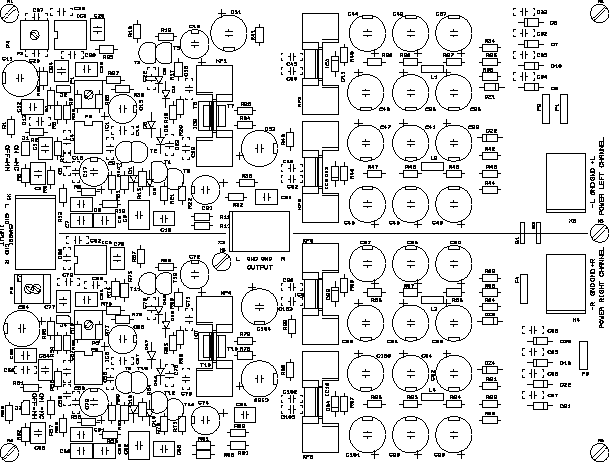
The picture shows the component print of the PCB. Of course you can't use it for anything except for an overview. Please download the pdf-file instead if you want to see the details.
The printed circuit board is made for two channels. It's possible to do this pcb by yourself. Just make the layout as the schematics. As you can see I have done it. The pcb have groundplane on the upper side (not shown in pictures) which is essential in order to get good results. I haven't made it easy for switching pickup. I gather you will use only one type and also trim for this type.
The solder side
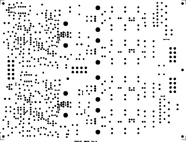
The picture shows the solder side of the PCB. Of course you can't use it for anything except for an overview. Please download the pdf-file instead if you want to see the details.
Almost everyone of the traces are on the solder side. The groundplane is very covering, only a few traces on the component side.
The component side
The picture shows the component side of the PCB. Of course you can't use it for anything except for an overview. Please download the pdf-file instead if you want to see the details.
Almost everyone of the traces are on the solder side as you can see. The groundplane is very covering, only a few traces on this side.
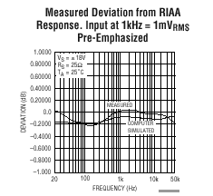
The RIAA correction curve
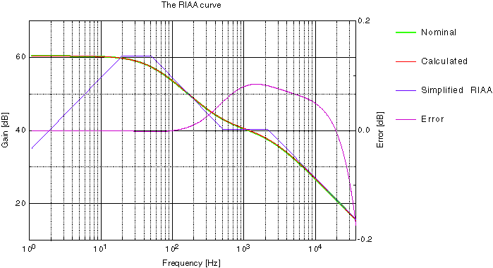
The diagram above shows the nominal and the calculated RIAA curve. The green curve is invisible because it lies almost exactly on top of the red one. If you look at the error curve, down below, you see why.
The diagram above shows the response curves for both RIAA equalization, and the IEC modified version. The latter was not very popular, maybe because it represented a loss of bass (-3 dB ref RIAA at 20 Hz) or was it introduced too late?
RIAA time constants
The time constants that provide RIAA equalization are:
Low Frequency = 3180 us (50.05 Hz)
Mid Frequency = 318 us (500.5 Hz)
High Frequency = 75 us (2122 Hz)
The RIAA-amp has a 'not very flat' frequency response. The reason for this is purely mechanical and exists to give both the cutter and the pickup a fair chance the do their job. The cutter is like a microphone or a loudspeaker. If you apply constant voltage to a loudspeaker you will notice that the movement (amplitude) of the cone is constant below the resonance frequency and above it, it is reversed proportional. If you double the frequency the movement will be half.
With this in mind, the grooves will get gigantic for bass tones and microscopical for the high ones. If you make the grooves very small they will be very sensitive for dust.
The first time constant at 50 Hz is to limit the cutters and the pickups movements in the low bass region below 50 Hz. Above 50 Hz the groove is cut with constant mechanical amplitude. The cutter has a resonance at 500 Hz. That is why the second time constant is at 500 Hz.
The 500 Hz knee suppresses the cutters resonance but you have still the dust problem. At 2122 Hz you will increase the treble and again cut the grooves with constant amplitude. This simple filter acts like a simple noise reduction.
If you remember the lessons from the schooldays you know that the output voltage is proportional to velocity. If the needle moves with a certain amplitude at 200 Hz and moves the same amplitude at 400 Hz you will get twice the output voltage. The signal increases with 6 dB/octave. This leaves us to design an amplifier with a filter that cut all frequencies with 6 dB/octave. But in the lowest region you don't have to cut.
It is this rather large amount of bass boost that accentuates the mechanical noise of a turntable, producing what is commonly known as "rumble". There is also the risk of low frequency feedback if the turntable is not capable of isolating the platter and tone-arm from the listening room environment. Timber floors and rigid suspension increase the risk of feedback.
The RIAA error curve
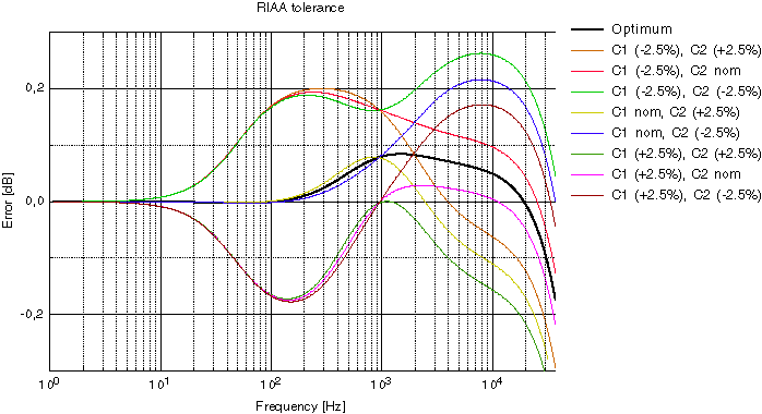
The diagram above shows the nominal error (black) and the maximum of the calculated RIAA curve. Valid for MM (moving magnet) mode.
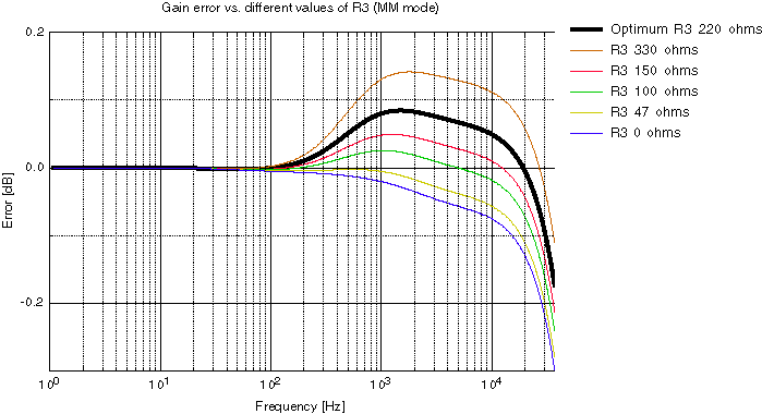
The diagram above shows the error with different values of R3, resistor which limits the lowest gain. Valid for MM (moving magnet) mode.
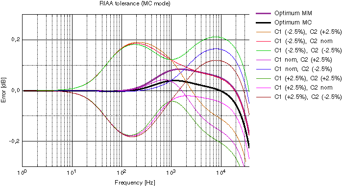
The diagram above shows the nominal error (black) and the maximum of the calculated RIAA curve. Valid for MC (moving coil) mode.
It's quite easy to achieve a very accurate RIAA correction curve. If you use 2,5% capacitors you should statistically achieve a very accurate RIAA-curve. I think the maximum error will be 0,2 dB and the typical less than 0,1 dB. I have derived the formulas and put them into a spreadsheet. Send me a mail if you want this Excel-file (version 8, Office 98). The nice diagrams above are made by the excellent program 'pro Fit' from QuantumSoft, www.quansoft.com.
The formulas are written with the freeware MathMagic from www.mathmagic.com

The simplified RIAA amp look like this. R4 together with R1+R2+R3 determines the DC-gain.
More text to come......
Build directions
Click on the picture to get a larger view. The printed circuit board of the QSX Mark III Amplifier.
Before you build, take a look at possible component selections. You can choose from two different output stages, chopper stabilized DC-servo, regular DC-servo or trimpotentiometer.
Start with the power supply
Solder in all (check first which passive parts you need) low passive parts (also diodes) for the whole amp. Wait with transistors, regulators, IC's and heatsinks. Notice which parts which are associated the bipolar output stage and with the integrated buffer.
Mount the regulators on the heatsinks. Only the negative regulator, 7915 need to be isolated from the heatsink. You will need a bushing, see the picture below, in order to isolate the screw from the tab. I recommend silicone rubber. There is nothing wrong to use mica washer or Kapton film (orange, very thin). Mount the regulators first at the heatsink, then mount the heatsinks at the pcb.
When the regulators are in place, solder in all big electrolytic caps, even those located at the amp.
Apply voltage to one channel at the time. Check that the voltage is plus 15 volts and minus 15 volts. Suitable measurement points are IC1, pin 7 and 4. Do the same thing with the other channel. Disconnect the supply voltage and make sure that all of the caps are completely discharged. The check the voltage in the IC1, pin 4 and 7. It must be less than 0,6 volts! This is only a precaution.
The output stage
Decide which type of buffer you are going to use, bipolar discrete or integrated.
The bipolar (BJT) output stage
Click on the picture to get a larger view.
The following parts are associated with the bipolar buffer: R18-R24, R67-R73, T3-T8, T11-T16, D3-D6, D15-D18, C22, C23, C75 and C76. The transistors have to be isolated from the heatsink.
The transistors have isolated holes so you don't need bushings. I recommend silicone rubber. There is nothing wrong to use mica washer or Kapton film (orange, very thin).
The monolithic (LT1010) output stage
Click on the picture to get a larger view.
I recommend the buffer as output stage. It costs a little bit more but the performance is higher, distortion lower. The following parts are associated with the bipolar buffer: R16, R17, R65, R66, IC2, and IC7
The buffer needs to be isolated from the heatsink. You will need a bushing, see the picture, in order to isolate the screw from the tab. I recommend silicone rubber. There is nothing wrong to use mica washer or Kapton film (orange, very thin).
DC-servo
You can choose from four options:
- Chopper stabilized operational amplifier with external auto-zero caps, MAX420, R25-R29, R74-R78, C24-C30, C77-C83, IC3 and IC8.
- Chopper stabilized operational amplifier with internal auto-zero caps, MAX430, R25-R29, R74-R78, C24, C25, C28-C30, C77, C78, C81-C83, IC3 and IC8.
- Conventional precision operational amplifier, R25-R29, R74-R78, C24, C25, C28-C30, C77, C78, C81-C83, IC3 and IC8 (OP07 or similar), P3, P7 or P4, P8, depending on chosen opamp.
- Plain trim potentiometers, P1, P5 or P2, P6, depending on chosen opamp.
All opamp choices are good but they are listed in performance order. I don't recommend trim potentiometers but I have made room for them anyway.
The Class A circuit
You can choose from three options:
- JFET, current source, T1, T9, R14 and R63. The value of these resistors need probably adjustment, higher value, 500 ohms or higher.
- BJT, current source, T2, T10, R14, R15, R63, R64, D1, D2, D13, D14
- Plain resistor, R14, R63 connected directly to the output. Suitable value 6.8-10 kohms.
The class A circuit can be omitted but it makes most benefit when the load from the opamp is small like when you use the LT1010 buffer.
The RIAA network
I have made the pcb so you can use the original Linear Technology design or my own.
You can choose from two options:
- The original Linear Tech design, without DC-servo. Compare with the datasheet and the schematics and check for which parts you have to use and also the parts which need changed values.
- My version, De Luxe! C6-C10, C31, C59-C63, C84, R4, R6, R8-R12, R32, R33, R53, R55, R57-R61, R81 and R82.
Omit R5, R7, R13, R54, R56, R62, C3-C5, C11-C13, C56-C58, C64-C66
Input filter
If you don't have any RFI problems, replace the R2, R51 with a jumper. R1, C1 and R50, C54 maybe need to be adjusted. Consult the datasheet of your MM pickup. If you are planing to use MC pickup, the load is R3, C2 and R52, C53. The capacitor for the MC load is not very critical, so I've heard.
The operational amplifier, the final part
Solder in only IC1 and IC6. Use IC sockets for test purposes only. If you use sockets permanently, use high quality ones with "tulip" contacts. I recommend not to use IC sockets. Short the input to ground or place a jumper at J1 and J3.
Check one channel
Apply supply voltage just this channel. Measure the output DC voltage. Should be ZERO with a MAX420 opamp and less than 2 mV with a regular opamp. Just to be sure, check the supply currents. Use R41 and R49 as current shunts. The current value should be ????
Check the other channel
Apply supply voltage for both channels. Measure the output DC voltage. Should be ZERO(!) with a MAX420 opamp and less than 2 mV with a regular opamp. Just to be sure, check the supply currents. Use R90 and R98 as current shunts. The current value should be ???? Connect a pick to the input. The amp should work now!
The whole pcb
Click on the picture to get a larger view.
The complete phono amp with all components soldered in. The left channel has a bipolar output stage and the right channel has an integrated buffer as output stage. This is only for the picture taking. I have also listened to the amp different output stages, can't hear the difference. I guess that LT1010 is slightly better than the bipolar stage.
Listening experience
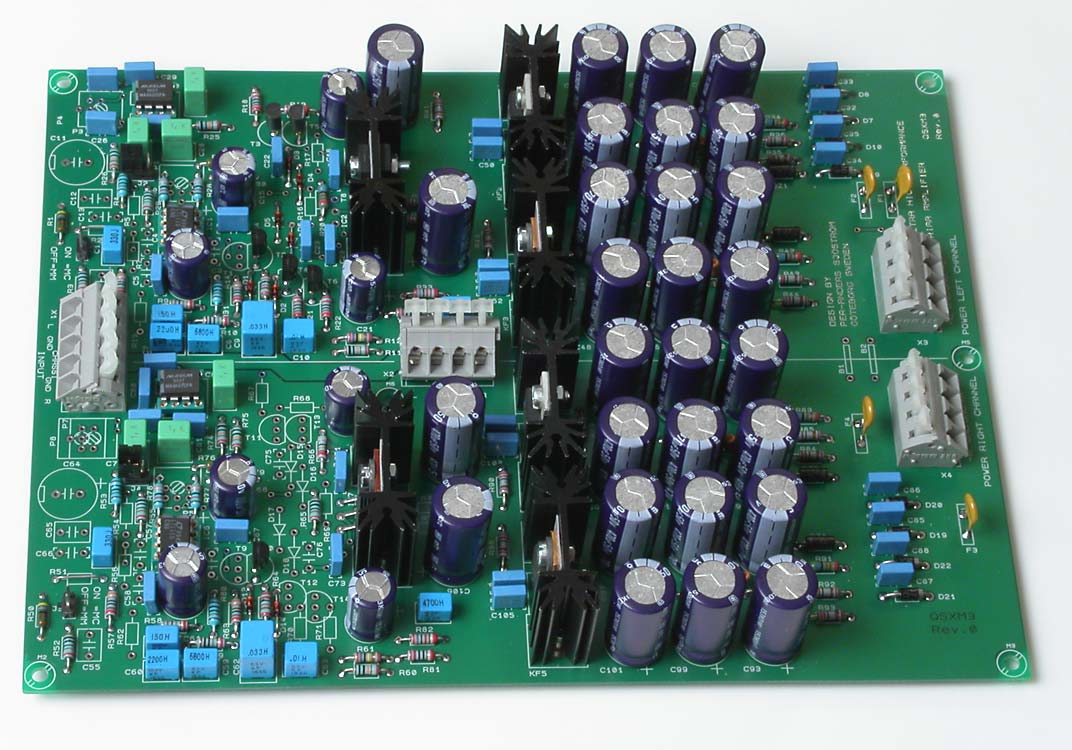
Click on the picture to get a larger view. The printed circuit board of the QSX Mark III Amplifier.
Why is it so important with the phono amplifier in order to get good sound quality?
See the page about QSX Mark II.
How does this particular amp sound? First of all, I'm amazed how similar this one sounds compared to my "monster". I have listened to this amp rather much now, mostly with headphones connected directly to the output. The amp can drive headphones at very high levels with a crystal clear sound.
It's a pure pleasure to listen to my old (but not worn out) vinyls. The bass is surprisingly firm and deep. The mids are very detailed "this haven't I heard before"-like. The treble sounds also good and the "clicks" aren't so clear. I think this is caused by the fast amp, high open-loop gain (creates descent feedback at all frequencies) and the high current output stage. The amp can take high frequencies into low impedance load without choking.
What is the difference between the transistor buffer (BD139/BD140) and the monolithic one (LT1010). Very little, in fact I can't hear any difference. Transistors are cheaper but the buffer is more advanced. I gather also that LT1010 can be a little harder to get compared to regular transistors. I recommend the LT1010 as output stage.
Technical data
| Frequency response according to the RIAA curve: | 20 Hz - 20 kHz, within 0,1 dB |
| Equivalent input noise: | 120 nV |
| Signal to noise ratio: | 101 dB, MM pickup 81 dB, MC pickup |
| Dynamic headroom: | 134 dB, MM pickup 114 dB, MC pickup |
| Distortion: | < 0,001 % |
| Slew rate: | 20 V/us |
| Step response: | Perfect without overshoot |
| Gain: | 100 (40 dB) MM pickup |
| Input impedance: | 47 kohms// 470 pF (0-270 kohms//20 pF and up, limited only by physical dimensions , user selectable) |
| Output impedance: | 600 micro ohms without output filter |
| Output current: | 150 mA, LT1010 buffer 1 A, BD139/BD140 buffer |
| Power bandwidth at 10 Vrms: | 0 Hz - 190 kHz, -3 dB |
| Dimensions: | 215 x 160 mm (8.5"x 6.3") |