JSR-02 The Sjöström Super Regulator
Click on the pictures to get a larger view.
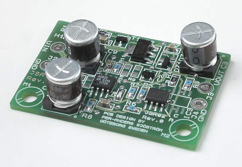
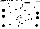
The component side. The pcb is rather small.
Some background can be found in my JSR-01 project.
This design is based on my JSR-01 project and the goal was to make the pcb smaller than the JSR-01 project. Therefore I have removed the preregulator because I think this regulator will be fed from a regulated voltage source.
Interesting features
- Extremely low noise.
- Very low output impedance in the audioband.
- Small.
- Easy to change voltage, also to negative voltage.
- Well-known and well-tested in serious applications.
- LM431 reference but I have made markings for anode, cathode and reference so it will be easy to mount any other 2- or 3 pin device like LM329.
No pcb's available
The last pcb's are now sold and I won't order more unless demand will arise.
The design
This design has very interesting features
The design is based nearly to 100% of the original super regulator. My contribution is transferring it to SMD and making the pcb universal negative/positive versions.
The schematics
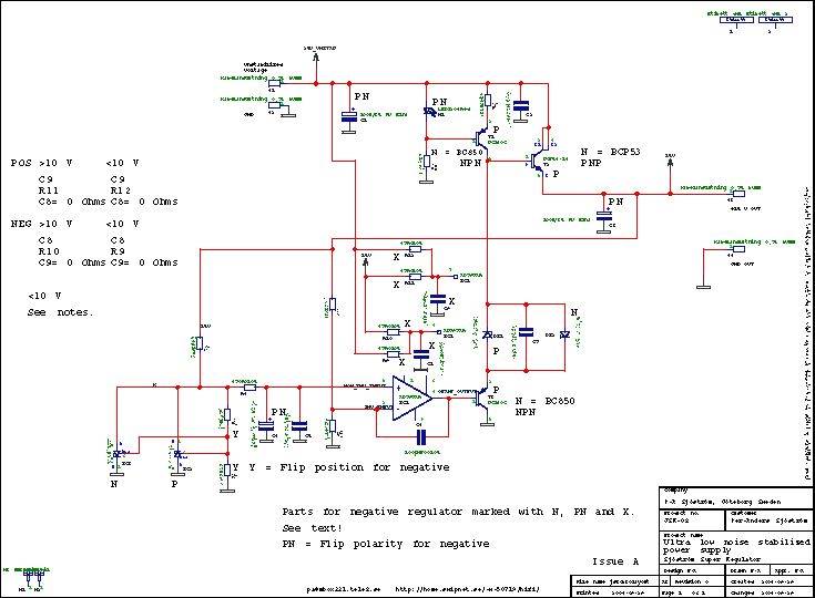
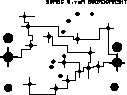
Click on the picture to get a larger view. The picture shows the schematics of the amp. Of course you can't use it for anything except for an overview. Please download the pdf-file instead if you want to see the details.
I recommend that you download the schematics and print it so you can follow the describing text more carefully.
Circuit description
The reference
As reference I have chosen to have maximum flexibility. Virtual any reference will fit as long as the voltage is above the common mode limit for the used opamp. 2.5-7 V will work and in some cases also 1.2 V. I have used LM431 in SO08 and this very cheap reference is rather good, although not as nearly as good as LM329 but much, much better than a regular zener diode (which also can used). As a little help if you use some other reference I have written
R(Ref), A(Anode) and C(Cathode) so you can connect almost any reference. The LM431 can be used for negative voltage just by turning it around but you will need a double footprint. Please notice that the resistors which are setting the reference voltage must be interchanged, R4 and R5 swap it's positions for negative voltage. R3 is carefully selected and may be changed if especially lower voltages are to be chosen. See instructions for this.
The reference voltage is filtered by R6 and C4, C5 in order to remove the noise and as a side effect you will get a smooth startup. R6 should optimally be R7 and R8 in parallel but I consider this not extremely important. You can either choose 499 ohms or simply solder two 1 kohms on top of each other. If you have matched input impedance's you will minimize the input offset and also the drift with temperature (not very important in audio applications). It may also be good when it comes to common mode rejection.
The opamp
The opamp can be almost any type as long it's not too fast, faster than the output stage. The maximum speed of the opamp at unity gain is around 30-40 MHz. The AD825 has the bandwidth of 34-37 MHz at unity gain and the AD797 has unity gain bandwidth of approx. 30 MHz. If extremely low noise is important AD797 might be suitable but if "low" noise is sufficient I think any good audio opamp will do, like AD8610, OPA134 etc. Even good old NE5534 may work but I haven't tested this opamp. The only thing you must think of is the common mode limits for the inputs of the opamp. At start-up it's important that the opamp has predictable behaviour, especially sensitive is this for a negative regulator.
At the moment only AD797 and AD825 are tested for 5-14 volts, both positive and negative output voltages. AD797 is not a optimal choice becasue of the restless phase behaviour over 1 MHz. As I see it AD825 is a very good choice if you want a really fast regulator and at the same time a good behaviour.
Power for the opamp
Since the pcb is made both for positive and negative voltages the opamp must have different connections for the power supply voltage, pin 4 and 7 at the opamp. You can either take the power from the output or before the pass transistor T2. What you choose is dependent of used opamp and how low the minimum supply voltage is (see the datasheet for this parameter). Minimum voltage for AD797 is 10 volts so if you want to be really sure you must feed it from the unregulated side if you want less than 10 volts out. Parts which are involved in this are R10-R13 and C10, C11.
Positive regulator, power from the output
R11 = 47 ohms
C9 = 100 nF
C8 = Tin jumper
Negative regulator, power from the output
R10 = 47 ohms
C8 = 100 nF
C9 = Tin jumper
Positive regulator, power from the unregulated side
R12 = 47 ohms
C9 = 100 nF
C8 = Tin jumper
Negative regulator, power from the unregulated side
R9 = 47 ohms
C9 = 100 nF
C8 = Tin jumper
The feedback network
The feedback network is very simple, only R7 and R8. The values of the feedback resistors should be a low as possible considering the max power dissipation. It serves to purposes. The first is to create a voltage divider with good high frequency properties (avoiding unstability) and also to draw current out of the pass transistor, T2. If current flows all the time also the output impedance can be kept extremely low. It's also important for stability reasons.
The output voltage is determined by the reference voltage * (R7/R8 + 1)
The output stage
The output stage is rather unusual. Normally you have only one emitter follower, maybe together with a driver transistor forming a Darlington transistor. This type of output stage is rather slow. To speed things up the driver transistor is changed to a class A emitter follower as the driver for the pass transistor. The load of the emitter follower (T3) is a current source formed by a reference voltage, the LED H1 (makes a nice glow) and R1 together with T1. The current through the LED should be 1-3 mA. If you want very low voltages you must change the value of R1.
The driver is also a bit backwards. This creates a very special and also very important feature, the possibility to a safe power up of the opamp. The output stage deliver max output voltage when the opamp is inactive. This makes the opamp come alive. The zener DZ1 (or DZ2) increases the startup voltage and creates also a necessary DC shift so the output of the opamp works at ideally at half the output voltage. This zener voltage must be decreased when lower output voltages are wanted. For 5 volts it's sufficient with a diode in the forward direction, creating only 0.7 volts. T3 is added compared to Walt Jung's original (but Mr. Kaneda had it) and unloads the opamp from the drive currents. C7 takes down the impedance of the zener.
No short circuit limiting
I have increased the current of the driver T1 and T2, for higher speed but this makes also the regulator more vulnerable against short circuit so I suggest you are careful when you are connecting.
Capacitive load and C19
The faster opamps you have, the more sensitive against capacitive load the regulator will get, meaning low loss capacitive load. The regulator has a minimum load of 0.3-0.5 ohms and if you have a 100 nF connected very close to the output transistor you can get an impedance lower than 0.5 ohms. This frequency will be at 3 MHz. Therefore the C9 must not be too "good". In fact a "normal" cap is sufficient and if you choose a low impedance cap you may experience unstability. If you use a fast opamp, it simulates a cap rather high up in frequency so serious decoupling this close to the output transistor isn't necessary but if you only have 30 mm wire the regulator can take 100 nF or more. The short wire creates a small inductance which is sufficient in order to limit the lowest impedance.
Build directions
....more to come.....
Test
....more to come.....
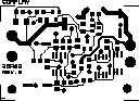
The PCB layout
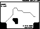
The component print
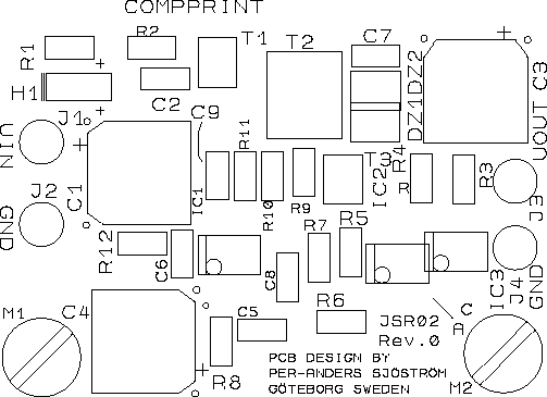
The picture shows the component print of the PCB. Of course you can't use it for anything except for an overview. Please download the pdf-file instead if you want to see the details.
The printed circuit board will be made of 50 um thick copper and has a groundplane on the solder side.
The component side
The pictures show from the left: the component side, the solder side, the groundplane mask (black areas are not groundplane) and last the thermo pads of the PCB. Please download the pdf-file instead if you want to see the details.
Most of the traces are on the component side.
Technical data
| Operating voltage: | 9-35 V, less current at high voltage in. |
| Output voltage: | 5-30 V |
| Hum and noise at full output current: | Down to 1 µV or below depending of component choices |
| Max current: | Approx 150mA peak |
| Max continuous current: | Approx 100 mA depending of ambient temperature and mounting. |
| Dimensions: | 41,9 (1.65") x 30,5 (1,2") mm |