Circuit description
The rectifier
The full-wave rectifier bridge is built up by four 1 ampere or 3 ampere diodes (D1 to D8). Each diode has a series resistor in order to reduce harmonics in the current. 600 mW or 5 W types will fit. The resistor value should be 0.5 to 2 ohms, not too much.
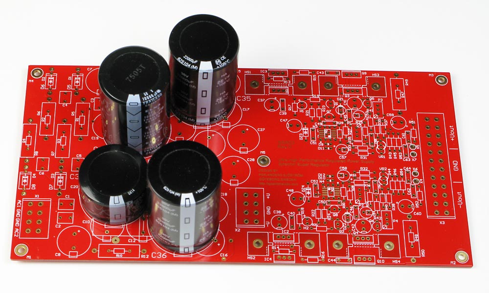
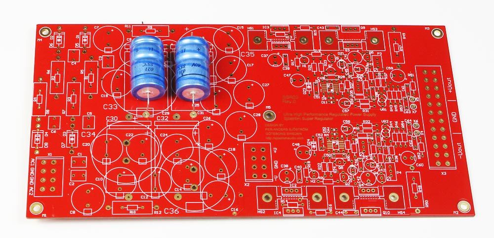
The first part of the smoothing is managed by C7/C8 followed by an another section consisting of R9, C9, C11, C13, C15, C17, C19, C21, C23, C25 and C27 and the corresponding parts for the negative voltage. The pcb has also room for 10 mm snap-in caps or axial caps.
Click on the picture to get a larger view.
10 mm snap-in capacitors. A few different sizes can bee seen in the picture, only for demonstration.
Click on the picture to get a larger view.
Axial capacitors, here Philips/NXP. You see also that bigger types will fit. Those at the picture were some caps I had in my drawers.
Unstabilised voltage
From connector X2 (in the middle of the pcb) you can feed things like relays which don't need ultra clean voltage.
The pre-regulator (positive side)
The first part is the pre-regulator (IC1), which has a rather odd connection. The sensing network, R13 and R15 is not connected to ground as usual. It's connected to the output so the LM317 regulates the voltage across the pass transistor Q3. The purpose of this is to create a constant voltage drop over this transistor. With this connection you will get a more flexible minimum input voltage which is 2.5 volts (according to the values of R13 and R15) plus the minimum voltage across the LM317 which is 2-3 volts. In total you will need approx. 5 volts more than the regulated output voltage.
The IC1 is the normal location for the LM317 and a heatsink will fit, 1, 1.5 or 2 inch high. You can also mount the regulator in IC3, then you can mount the part on a smooth surface. In case you do that the part should be mounted from the solder side and soldered on the component side. Pay attention how you should turn the device.
You can omit the pre-regulator, just short pin 2 and 3 IC1 and don't mount the R13 and R15. The pre-regulator will increase the power supply rejection ratio but unfortunately I no figures for this improvement.
The reference (positive side)
As reference I have chosen to have maximum flexibility. Virtual any reference will fit as long as the voltage is above the common mode limit for the used opamp. 2.5-7 V will work and in some cases also down to 1.2 V. LM431 and LM329 is supported. Other references will work but check the pinout first. The LM431 (thick outline in the silkscreen print) has four resistors R39, R41, R43, R45 and a trimpotentiometer P3 in order to trim the reference voltage. You can't trim the LM329.
The reference voltage is filtered by R35 and C55, C57 in order to remove the noise and as a side effect you will get a smooth startup. R35 should optimally be the value of the feedback network impedance, (R25+R27)//R31//R33. //= means in parallel.
If you have 1k+1k in the feedback you can for the R35 either choose 499 ohms or simply solder two 1 kohms on top of each other. If you have matched input impedance's you will minimize the input offset and also the drift with temperature (not very important in audio applications). It may also be good when it comes to common mode rejection. Since the whole design is placed on a groundplane I gather that high frequency problems are not so big so you must take this into account. R29 and C51 are parts for "just in case", to customize the frequency properties. Normally R29 is only a wire jumper or a low value resistor and C51 is omitted.
Fat outline (print on the pcb) is for LM431 and the thing outline is for LM329.
The opamp (positive side)
The opamp (N1) can be almost any type as long it's not too fast, faster than the output stage. The maximum speed of the opamp at unity gain is around 30-40 MHz. The AD825 has the bandwidth of 34-37 MHz at unity gain and the AD797 has unity gain bandwidth of approx. 30 MHz. If extremely low noise is important AD797, LT1012 and LT1115 might be suitable but if "low" noise is sufficient I think any good audio opamp will do, like AD8610, OPA134 etc. Even good old NE5534 may work but I haven't tested this opamp. The only thing you must think of is the common mode limits for the inputs of the opamp. At start-up it's important that the opamp has predictable behaviour, especially sensitive is this for a negative regulator.
At the moment only AD797 and AD825 are tested for 5-24 volts, both positive and negative output voltages. Others have tested LT1028/LT1115 with good results.
Input protection of the opamp (positive side)
D9 and D11 is input protection fo the opamp in case you can get differential voltages higher than the maximum ratings, for instance at short circuit conditions. Under controlled conditions you can omit these diodes since they introduce an extra capacitance at the input.
Power for the opamp (positive side)
You can either take the power from the output or before the pass transistor Q2. What you choose is dependent of used opamp and how low the minimum supply voltage is (see the datasheet for this parameter). Minimum voltage for AD797 is 10 volts so if you want to be really sure you must feed it from the unregulated side if you want less than 10 volts out. Parts which are involved in this are R5-R6 and C7, C8. The DZ2 must be used if the supply voltage is more than the maxium supply voltage of used opamp. The value of the zener should be lower than the maximum supply voltage of the opamp.
The feedback network (positive side)
The feedback network is R25+R27 as the upper part. R25 is normally a wire and is used for trimming purposes. R31 in parallel of R33 is the lower part of the feedback and R31 is for trimming also. P1 can also be used if you want a variable output voltage, recommended if you use a fixed voltage reference like the LM329.
C53 reduces the gain and by this increase of the feedback which also reduces the output impedance. This capacitor is hardly necessary in real life (if the gain is 2) but if you want lower output impedance you should use it. The values of the feedback resistors should be a low as possible considering the max power dissipation. It serves two purposes. The first is to create a voltage divider with good high frequency properties (avoiding unstability) and also to draw current out of the pass transistor, Q3. If current flows all the time the output impedance can be kept low. It's also important for stability reasons.
The output voltage is determined by
Vout = Vref*(((25//P1)+R27)/(R31//R33)+1)
The output stage (positive side)
The output stage is rather unusual. Normally you have only one emitter follower, maybe together with a driver transistor forming a Darlington transistor. This type of output stage is rather slow. To speed things up the driver transistor (Q1) is changed to a class A emitter follower as the driver for the pass transistor (Q3). The load of the emitter follower (Q1) is a current source formed by a reference voltage, the LED H1 (makes a nice glow) and R17 together with Q1. The current through the LED should be 1-3 mA. If you want very low voltages you must change the value of R17. A side effect of the LED H1 is that you will get an indication when you have enough input voltage and you have a stable output voltage.
The driver is also a bit backwards. This creates a very special and also very important feature, the possibility to a safe power up of the opamp. The output stage deliver max output voltage when the opamp is inactive. This makes the opamp come alive. The zener DZ1 increases the startup voltage and creates also a necessary DC shift so the output of the opamp works at ideally at half the output voltage. This zener voltage must be decreased when lower output voltages are wanted. For 5 volts it's sufficient with a LED in the forward direction, creating only 1.6 volts. Q7 is added compared to Walt Jung's original (but Mr. Kaneda had it) and unloads the opamp from the drive currents. C45 takes down the impedance of the zener.
No (or limited) current limiting .... or have it (positive side)
I have increased the current of the driver Q1 and Q3, for higher speed but this makes also the regulator more vulnerable against short circuit so I suggest you are careful when you are connecting. It is possible to destroy the regulator but the LM317 (IC1) has current limitation 1.5 amps, still you must be carefull. Adding short circuit protection will increase the output impedance if you not implement an advanced circuit which requires lot's of pcb space. If you want a simple current limitation you change the wire at R47 to a resistor and also mount Q5. The current limit is set to 0.65/R47.
Capacitive load and C59 (positive side)
The faster opamps you have, the more sensitive against capacitive load the regulator will get, meaning low loss capacitive load. The regulator has a minimum load of 0.3-0.5 ohms and if you have a 100 nF connected very close to the output transistor you can get an impedance lower than 0.5 ohms. This frequency will be at 3 MHz. Therefore the C59 must not be too "good". In fact a "normal" cap is sufficient and if you choose a low impedance cap you may experience unstability. If you use a fast opamp, it simulates a cap rather high up in frequency so serious decoupling this close to the output transistor isn't necessary but if you only have 30 mm wire the regulator can take 100 nF or more. The short wire creates a small inductance that is sufficient in order to limit the lowest impedance.
The "sense" connections (positive side)
The sense connections are a bit overkill but if anyone wants these I have added this feature. The sense function is mainly to subtract or eliminate the losses in the power wires, which won't be especially large. It's just milliamps. If you want this feature make sure that the sense wires are close to the power wires so instability can be avoided. If you don't want to use this feature, just put two tin jumpers on the pcb solder side, marked J1 and J2. If you are sure that you never will use the sense function you can also omit R51, R53, C61 and C63.
