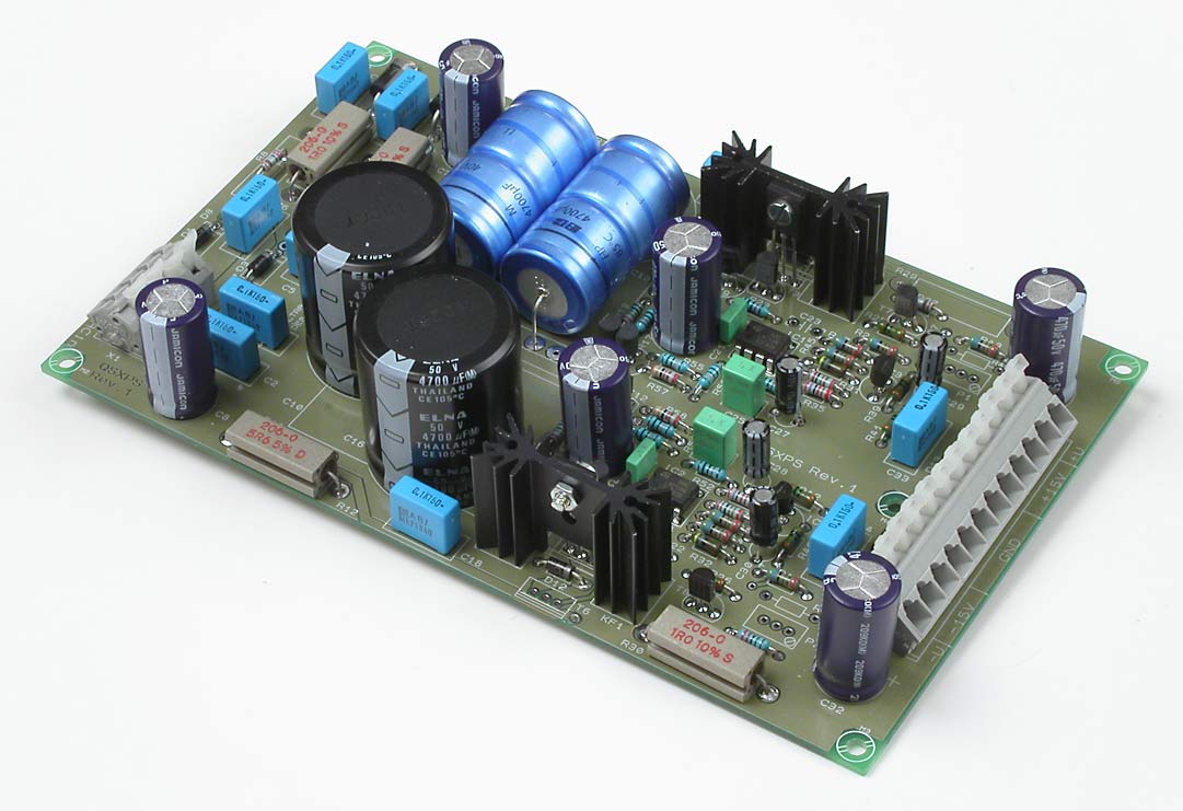
QSXPS - The extreme power supply
Click on the picture to get a larger view.
This power supply design did I make for the DAC and for the new ultra extreme RIAA amp .
This design has very interesting features:
- Extremely low output noise.
- Very low output impedance in the audioband.
- Easy to change the output voltage
- High performance rectifier bridge built by discrete parts
- Well-known and well-tested in serious and demanding applications.
- LM431 as reference.
- Extra trimming resistors for tuning the output voltage.
- Frequency compensation for the opamp added as an option. By that you are more free of choosing opamp.
- All resistors 10 mm between the holes so it is possible to use a cut and bending machine for those parts.
- Current peak limiting resistor after the rectifier bridges. Reduces the harmonics in the raw voltage.
- Not particularly hard to make to independent regulators. Convenient if you want to make two positive voltages. This is not tested and verified.
The design
The design goal was not to use expensive or extreme parts and the performance should be quite outstanding! If you look at technical data maybe you agree. But remember one thing: This power supply is designed to work with known loads. It can be used for any application which needs quite supply voltage. There are also lot's of room for tweaking and trimming and alternative parts such as standing smoothing caps (which are substantially more expensive than the blue BC Components). I have made options for more current and power. You can also change both opamps and voltage reference. The pcb is now made of real thick copper, around 95 um or 2.7 oz.
The schematic
The schematic, page 1 of 3, the positive regulator.

The picture shows page 1 of the schematic. Of course you can't use it for anything except for an overview. Please download the pdf-file instead if you want to see the details.
The schematic, page 2 of 3, the rectifier and smoothing capacitors.
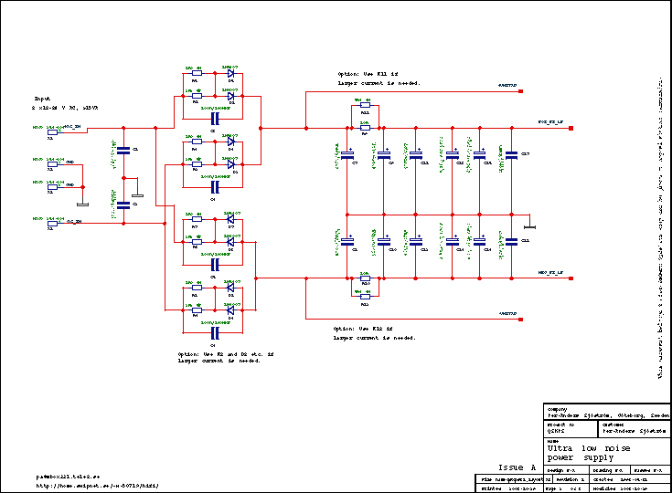
The picture shows page 2 of the schematic. Of course you can't use it for anything except for an overview. Please download the pdf-file instead if you want to see the details.
The schematic, page 3 of 3, the negative regulator.
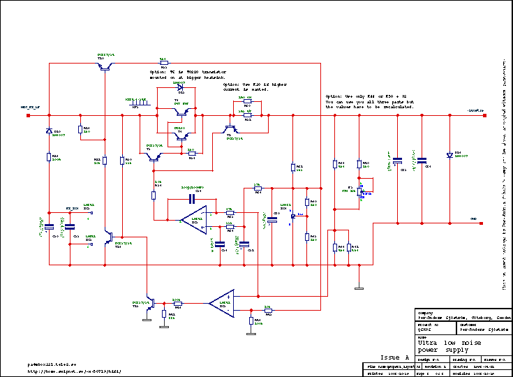
The picture shows page 3 of the schematic. Of course you can't use it for anything except for an overview. Please download the pdf-file instead if you want to see the details.
The design is rather unconventional but not very complicated if the different sections are identified. It has similarities with the Jung Super Regulator (as it has been called lately by the diy people) but was designed long before Walter Jung published an article in Audio Amateur, issue 1 and 2, 1995.
The major difference is that the opamp gets it's power from the unstabilized side and the smoothing capacitance is huge, 470µF for an opamp which consumes 2 mA. This design requires opamps which are "rail-to-rail" or almost which LM258/LM358 is. This is crucial at startup. The LM258/LM358 can handle signal near the negative supply pin, pin 4 but not very well signals at "top". Luckily the opamp can start, especially with help from the startup circuit.
The PCB layout
The component print

The picture shows the component print of the PCB. Of course you can't use it for anything except for an overview. Please download the pdf-file instead if you want to see the details.
The printed circuit board is made for one or two channels if you use it for QSX Mark II.
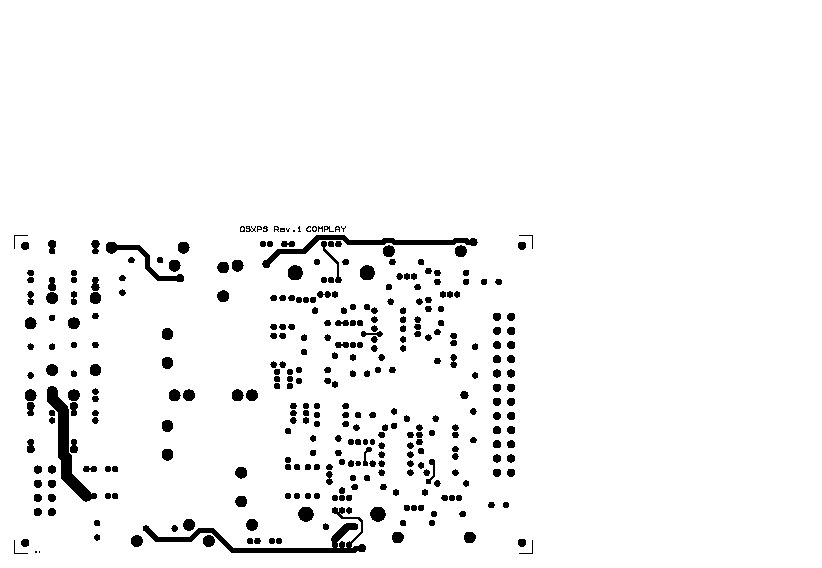
The solder side
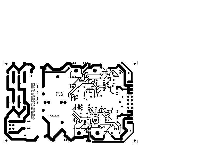
The picture shows the solder side of the PCB. Of course you can't use it for anything except for an overview. Please download the pdf-file instead if you want to see the details.
Everyone of the traces are on the solder side. The groundplane is very covering, no traces on the component side.
The component side
The picture shows the component side of the PCB. Of course you can't use it for anything except for an overview. Please download the pdf-file instead if you want to see the details.
Everyone of the traces are on the solder side as you can see. The groundplane is very covering, no traces on this side.
Technical data
| Output voltage: | ±15 V, ±0,001 V (5-25 V) |
| Max output current: | ±300 mA (to 3 A if parts are changed) |
| Output impedance: | 10 micro ohms |
| Hum and noise: | 16 uV at full output current |
| Dimensions: | 112,4 (4.425") x 182,9 (7,2") mm |