Circuit description
The amp consist of two main parts, a preamp and a correction amp.
The preamp (see above and pdf-files ) has very low noise and an extremely flat frequency response, up in the megahertz-region. The input impedance is determined by the input bias servo. With the chosen resistor values the input impedance is 270 kohms. It's very easy to tailoring the input characteristics in order to fit any pickup. With resistors and capacitors, you can choose the input characteristics in the way you want.
The RIAA-amp amplifies the signal even more and then correct it according to the international RIAA-curve. The bass drop under 20 Hz isn't implemented. Unfortunately the input impedance of the RIAA-amp is low, only 680 ohms, but this compensates with the extremely low output impedance of the preamp, only 800 microohms.
In order to get an extremely linear and extremely low distortion design I have taken a couple of measures:
- Symmetrical design
- No capacitors in the signal paths
- Cascodes in the input stage and in the high gain stage
- Buffered cascodes with emitter followers
- Possibility to use ultra low noise transistors
- High speed output stage
- Advanced input bias servo with chopper stabilized or conventional opamp
- Totally DC-coupled together with DC-servos and input bias current servo
- Many decoupling capacitors and EMI-filters
- Professional quality printed circuit board with groundplane
Symmetrical design
The whole amp is completely symmetrical (not entirely because of the fact that NPN and PNP never will be their exact opposites) with help from PNP- and NPN-transistors. The benefit of a symmetrical design is lower distortion and I like symmetrically designs, just by the looks.
No capacitors in the signal paths
Two DC-servos eliminates the input offsets, which always are present. No capacitors are the signal path. Therefore the offset voltage is about 2000 times higher than in a normal AC-coupled amp. The residual offset comes from the DC-servo and the opamp. The offset voltage is the DC-voltage at the output when you have no signal applied to the input. It comes from deficiencies in the input stage times the total DC-gain. In my case it is some millivolts times 2000. The offset comes from differences in the input transistors characteristics, temperature, DC-gain etc. It's impossible to make two identical transistors. There is always a difference between two transistors. You can minimize the defect by having two or more transistors on the same chip. Examples of very good matched monolithic transistor pairs are SSM-2210 (not available anymore) and same type in metal can MAT02 (NPN) and the PNP-types SSM-2220/MAT03. The difference is only DIL08 plastic package and TO-78, metal can....and the price I must add!.....1,5 vs 10 dollars!
Is there anyone who knows if there are alternatives to MAT02/03?
Input bias servo
To reduce the output offset voltage further the amp has also a circuit which injects DC-current to the input. The input currents are not negligible if ultra low noise transistors are used. If MC pickup is used and normal BCxxx transistors there is no need really for this servo but for MMs pickup it is. You can also use a low noise precision opamp also but then you must remove the zeroing caps. The zeners DZ9, DZ10 are only need when using MAX420 because this opamp can't take more than +- 15 volts as supply voltage. You can also use MAX430 which has internal zeroing caps.
Cascodes
The cascode stage is a very useful combination of two transistors. The benefits are two, lower distortion and dramatically extended frequency response. T27 and T29 is one of the cascodes. The gain is 20000(!) and the bandwidth 20 kHz. Maybe it's not that interesting to know why the stage gets faster, but it's true. But why does the distortion decrease?
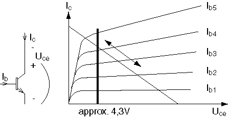
The bipolar transistor is a current driven device. You are only interested in input (base) current and output (collector) current. The picture above shows that the current gain is dependent of the applied voltage on the collector. If i.e. Hfe is 300 at 1 mA and 25V, it gets 350 at 35 volts. The current gain isn't a constant parameter. It changes also if you change the base current. 10 uA base current generates 1 mA, 20 uA, 2,2 mA, 30 3,6 mA. The fact that the current gain isn't constant generates harmonic distortion. But the greatest "defect" is the sensitivity for varying collector voltages.
If you take out the output signal at the collector with a help from a collector resistor, you'll get a signal that moves along the load line, see above. The graphical way of showing it is that the lines for Ib1, Ib2 etc. gets more separated at higher collector voltages, at the right. This is a sign that the current gain is higher than at the left (low collector voltages). Parallel, but maybe inclining, lines is a sign of constant current gain.
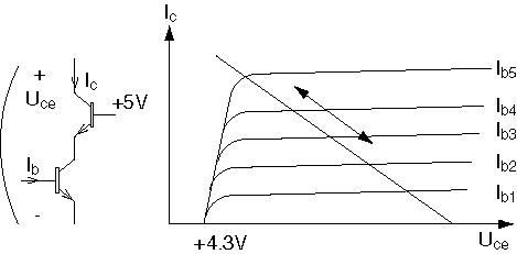
If you try to keep the collector voltage constant and in some way try to use the collector current you get interesting results. The "magical" load is the input of a base grounded stage. The base is at a constant potential with respect to signal ground. The input impedance of a such stage is very low, 25 ohms at 1 mA, 2,5 ohms at 10 mA. The base grounded stage isolates the first transistor from collector voltages variations.
The results of this are:
- Elimination of the Miller effect and therefore increases (extends) the frequency response dramatically
- Reduction of distortion
- Creates a super transistor with high gain, high voltage and high speed and also high power in some circumstances.
Advantage to use cascodes in an input stage:
- Faster input stage and therefore easier to feedback and to get a stable combination. The input stage should be as fast as possible.
- Possibility top use low voltage and low noise transistors and high supply voltage, especially important in power amplifiers.
Advantage to use cascodes in a high gain stage:
- Possibility top use low voltage and fast transistors together with high voltage ones and achieve high gain at high voltage swings.
- Low distortion
- Faster stage (sometimes an advantage)
Explanations of the specific design, the pre amp.
Please download all the schematic pages and print them out. It's much easier to understand what I'm talking about if you look at the circuits at the same time. I will only talk about the left channel and the upper half. The design is symmetrical and the two channels are identical.
The input filter
It's very important to tune the input impedance in order to achieve flat frequency response. If you choose to use the input bias servo (see page 7) the input impedance will be 270 kohms (R97) and if you choose not it's several megaohms (you can ignore it).
R1 together with R97 creates 47 kohms needed for most MM pickups and R3 is for MC pickups.
R2 together with C2 is an EMI-filter. In order to achieve the lowest noise possible R2 should be 0 ohm if you don't have any RF interference. If you have some trouble start first with:
- a wire with ferrite beads
- a bigger ferrite inductor with one or few windings
- an inductor 100µH to start with
- a resistor, 10-100 ohms (avoid due to increased noise, especially in MC mode)
Correct pickup load
It's important especially for MM-pickups to have correct load. Too little capacitance creates a sharp resonance peak at 8-20 kHz which can cause a sharp treble sound. The resistance is determined by R1 (MM), R2 (MC) and R97. The right capacitance is also important, especially for MM-pickups. 100-500 pF is normal values. Consult the pickup manufacturer for the right value. MC-pickup demands much bigger capacitance C2. I have chosen 10 nF. Normally MC don't need any input capacitor but to be sure, consult the datasheet of the pickup. With jumper J1 you can in an easy way change load. The best solution is to solder the jumper pins (and exclude the jumper itself) but I think the contact in the jumper is quite good.
The differential (input) stage
Current source (for the negative half) for the stage is DZ1 sets a 6.8 V voltage, feed through a LP-filter (R7, C3, C5) with reduces noise from zener and power supply and makes the amp start up nice when the power is switched on. The voltage drop across R7 is approx. 0.4-0.5 V. This makes a voltage across R9 of 5.65V. The current is therefor 1.45 mA divided in four equal parts through R17, R19, R21, R23 feeding the differential transistors (T5-T23, T7-T21, T9-T19, T11-T17) which can be separate components or monolithic and matched pairs.
T13 and T15 forms a cascode together with the lower transistor pairs. This type of stage extends the frequency response by a factor of at least 10. The distortion is also reduced. T3 creates a constant current and a constant voltage across R13 related to ground. The voltage is approx. 4.6 V. T13 and T15 are biased via R15 and smoothed by C11 and C15.
In order to get low noise the input transistors should not have any emitter resistor (no resistance between its emitters i.e. T5 emitter to T23 emitter).

The gain is (at room temperature 25°C) A = Ic * Rc* 0.040 * 1/2= 1.45*10-3 * (2200 + 680) * 0.040 *1/2 = 83 = 38 dB.
You can see that the frequency response is not flat. This is because I wanted to optimize the noise performance. Maybe there is some combination which is better but I haven't investigated that. You can probably use a little bit less gain in both the input stage and the high gain stage. There is no problem to lower the gain just in increasing it. When you increase the gain sooner or later you will get oscillations.
Noise improvements
The noise performance is the best at 100-300 µA and MM-pickup with BC550/560 transistors. 1 mA or more is the best for MC-pickup. If you use MAT02/03 the optimum current is approx. 1-5 mA. If you use MM-pickup it's also recommended to have 1 mA at least. If you choose to use MAT02/03 I recommend 1 mA through each transistor. Don't forget to lower the value of R25 and R31 and increase C7.
If you use transistors in parallel the noise is lowered by a factor of square root of 8 (= 2.8 = 9 dB).
Noise improvements with extra pairs:
| No of pairs | Factor square of | Factor | dB |
| 1 | 2 | 1.41 | 3 |
| 2 | 4 | 2 | 6 |
| 3 | 6 | 2.4 | 7.8 |
| 4 | 8 | 2.8 | 9 |
| 5 | 10 | 3.2 | 10 |
| 6 | 12 | 3.5 | 10.8 |
| 7 | 14 | 3.7 | 11.4 |
| 8 | 16 | 4 | 12 |
| 9 | 18 | 4.2 | 12.6 |
| 10 | 20 | 4.5 | 13 |
| 11 | 22 | 4.7 | 13.4 |
| 12 | 24 | 4.9 | 13.8 |
| 13 | 26 | 5.1 | 14.1 |
| 14 | 28 | 5.3 | 14.5 |
| 15 | 30 | 5.5 | 14.8 |
As you can see, the improvements gets smaller and smaller the more pairs you use. More than 4 pairs are not very wise. It's better to choose other components with lower noise.
The emitter follower after input stage and cascode
The emitter follower T25 decreases the effect of the load from the high gain stage T27 and T29. The result is mainly extended frequency response of the first stage. The second result is lower distortion. The main advantage of the emitter follower is increased phase margin and therefore better stability when the whole amp is feedbacked. The odds not to have oscillations increases.
The frequency response of the emitter follower is very high and also a little bit tricky to measure it. The value above is a guess.
The high gain stage
The important high gain stage is formed by T27 and T29. A minor local feedback is created by R35. The total gain is quite extreme, approx. 20000 times! The gain is lowered further with R37. The result is gain determined by R35/R37 = 3300 (70 dB). C17 creates a dominant pole in order to get a stable amplifier when feedbacked. The gain is very easy to adjust, just change the relationship between the mentioned resistance's. If the pre amp always shall work in MC-mode, it's possible the lower the capacitance's in order to get a faster stage and lower the distortion. An easy way to test how small the capacitance can be, apply square wave and trim for a perfect step response. The value of C17 is a compromise in order to use MM and MC pickups without any trimming, just changing a jumper.

The fast output stage
I have chosen cheap but fast small signal transistors to get a very fast output stage. Since the rated power is rather small and load is rather heavy (the feedback resistors) it's necessary to use three pairs. The feedback resistors have to have a low resistance in order to get the lowest noise possible.
The reason why I have a LED as bias voltage generator is, easy to get a stable bias current and low values of the emitter resistance's and therefor a low output impedance. Low impedance is important when driving low impedance loads in order to get low distortion. Oh, I forgot, LED looks cool! You don't have use red LED but if you change colour notice that the current will increase due to higher forward voltage. But this is not a problem, just adjust the emitter resistors (R43-R47, R82, R83) to a little bit higher value.
Test point
TP1 is a test point in order to be able to measure the pre amps characteristics in an easy way. The printed circuit board has groundplane and it's very easy to short down to ground when measuring and by that damaging the amp.
DC-servo
It's virtual impossible to get good DC-performance without some kind of servo (based on good opamps). The servo has some difficulties to be connected conventionally to the junction of the inverting input (base of T23 etc.) because of the low resistor values. The servo will consume a great deal of power but otherwise it's not a problem.
I have chosen to inject current inside the amp instead. Through R27, R29 a small current is either injected or drained. C9 makes sure that no audio signal goes into the servo and also that the servo not introduces any noise. The opamp IC1 should be a decent type with good DC-performance, slow and with low noise. The speed of the opamp should be not more than 1 V/µs. The opamp works as a non-inverting integrator. You should always have symmetrical component values in order to get a true integrator and also to get low offset caused by input offset currents of the opamp.
Input bias servo
Because the input stage has noticeable input current, an offset voltage is always present. If ultra low noise transistors are used, this servo is very important because of the high base current from the negative half. The PNP types of this transistor type has rather low current gain and the NPN-type rather high. This causes an unbalance in base currents. IC5 works a normal inverting integrator which strives to keep the output of the opamp at zero volts. The servo speed is very dependent of the pickup resistance. MC pickup creates a time constant of minutes and MM pickup creates time constant around one minute.
Feedback
The total gain (all of the separate diagrams combined) shown in this picture.
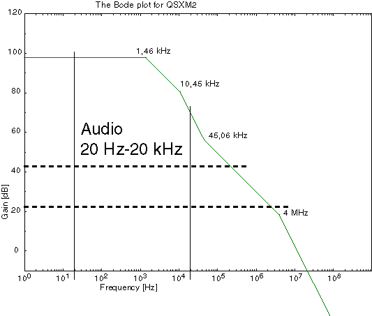
Long time ago when I made the original of the diagram, I made a mistake. I made the open-loop gain too high (not knowing). My goal was 100 dB gain but it became 108 dB. In real life the emitter follower is a substantial load together with the feedback network. Therefore the gain is a little bit lower.
Attention: Don't connect or disconnect the pickup when the amp is turned on! The servo creates a large spike which can damage your power amp, speakers, headphone!
The servo is slow in order to be able to work in background and not disturb the pickup signal in any audible way. My special kind of circuit attenuates the opamps inherent noise and to be sure it's a really low noise servo I have chosen an extreme chopper stabilized opamp. The special circuit makes the servo slow. With MC-pickup we talk about a minute or more to settle. With MM-pickup it's a couple seconds in settling time.
SMD types, alternative transistors
Long time ago (in 1986) when I first designed this amp it was very easy to get good hole mounted types of transistors but now it can be quite hard to get good transistors with high gain. It's rather easy though to get good surface mounted types. Therefore I have made room for SMD types in every transistor position. I have also included the possibility to use cheap transistor pairs (very small devices) and for matched ultra low noise matched pairs. SMD transistors aren't so hard to solder by hand but BC847BS/BC857BS are not suitable for newbeginners, only if you are VERY handy with the soldering iron.
The RIAA-amp
Most of the design is the same for the correction amp as for the preamp. The difference is only one transistor pair in the input stage, a single output stage and connected as an inverting amplifier. This amp is not so critical as the ultra low noise preamp. Here we don't need neither low noise performance or high current output. R84 serves as a simple short circuit protection and together with C53 it forms a LP-filter (EMI-filter). The cut frequency is 459 kHz. I think it's wise to have some protection against RF-interference. This filter can be omitted but leave the resistor R84 so you have short circuit protection. The output stage can drive a rather long cable with good results. I think at least 10 m or 30 ft is no problem.
This amp is a little bit slower than the pre amp because of the need to be stable at gain of 1 (no gain). C41 has a larger value than C17.
The RIAA-correction filter
The RIAA-curve and the circuit is explained here.
The capacitors for the RIAA-network should be high performing and with tolerance of less than 5%, preferable 2.5%. If you can't get hold of precision caps it's OK to measure up 5 or 10% caps. I think both polycarbonate and polyester will work rather well but I recommend polypropulene.
