The schematics, page 1 and 2.
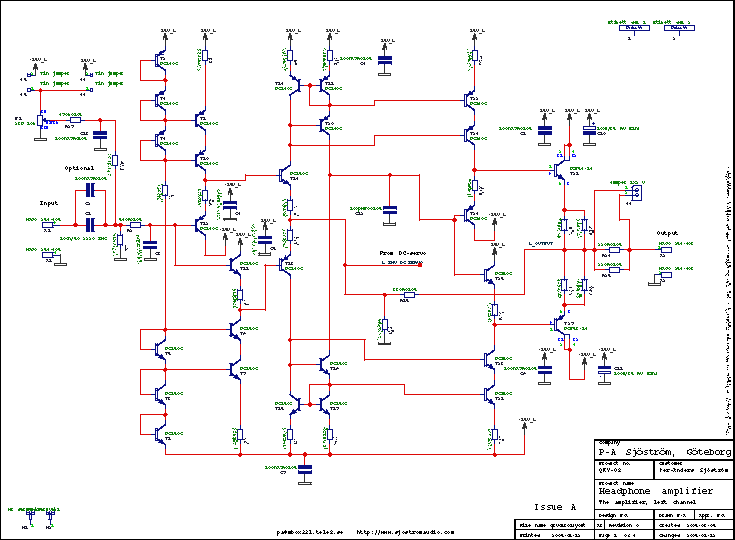
Click on the picture to get a larger view. The picture shows the schematics of the amp. Of course you can't use it for anything except for an overview. Please download the pdf-file instead if you want to see the details.
The text is for the right channel.
I have chosen to use current generators with cascodes as emitter loads. How much good the cascodes do is unknown at the moment. The only obvious disadvantage is a little bit reduced output voltage swing, otherwise only positive things, like less distotion and higher speed.
The current in the first stage (the input buffer) is set by T1, T3 and T2, T4 along with R4 and R5. I have transistors as diodes just to make it simpler when it comes to parts. The current is 0.65/560= 1,1 mA. The input stage of the amp is set by the relationship between R6/R10, and R7/R11, 10/2.2 = 4.5 => 5.3 mA. This current is then mirrored in the wilson current mirror, formed by T16, T18, T20, R8, R12 and T15, T17, T19, R9, R13. The resistors serves as local feedback which make the currents mirrors a little bit more linear.
The collectors of T19 and T20 creates a high impedance node and is also the output of the amp. This high impedance output must be buffered in order to useful. This is done with a diamond buffer. The current is given by the current in the mirror times R12/16 = 2.4 mA. The output stage runs in class A (which the whole amp does) 2.4 mA * R18/(R20//R22) = 10.2 mA.
My choice of currents is "average", because you both increase them och also decrease them. The max current is set by the max allowable power dissipation of the transistors. The small SOT23 types can take 310 mW or so and the SOT223, output transistors can dissipate 1.3 W but not in this application I imagine. More current mean slightly higher speed.
The input filter R2, C3 may be necessary if you are having trouble with RF interference. The values can be set to almost anything. The frequency is calculated by f= 1/(2*pi*R2*C3).
The performance is very good. See the technical data!
Interesting features:
- The pcb fits virtually any SOT23 small signal transistor and almost any SOT223 power transistor.
- The emitter loads have cascodes in order to increase linearity.
- SMD caps, including electrolytic caps.
- SMD parts which makes the buffer very small and thin.
- Input LP-filter if you have problems with RF interference, if not just omit it.
- Professional pcb with groundplane which establish good cooling and shielding.
The schematics, page 2
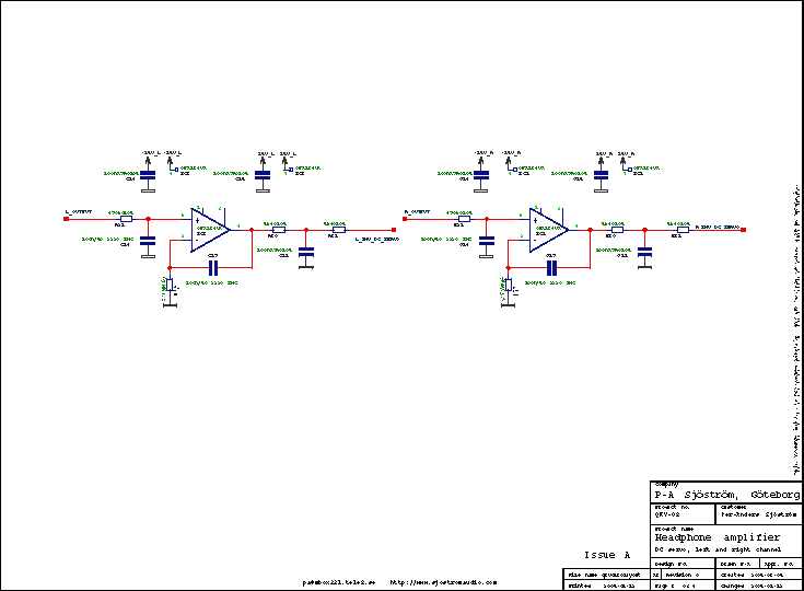
Click on the picture to get a larger view. The picture shows the schematics of the amp. Of course you can't use it for anything except for an overview. Please download the pdf-file instead if you want to see the details.
This is the DC-servo which is non-inverting and is a well-known design.
The schematics, page 4
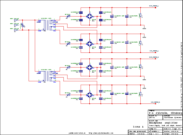
Click on the picture to get a larger view. The picture shows the schematics of the amp. Of course you can't use it for anything except for an overview. Please download the pdf-file instead if you want to see the details.
These pages show the design for the raw voltage. R58 is a varistor and is for supression of high voltage spikes.
The schematics, page 5 and 6.
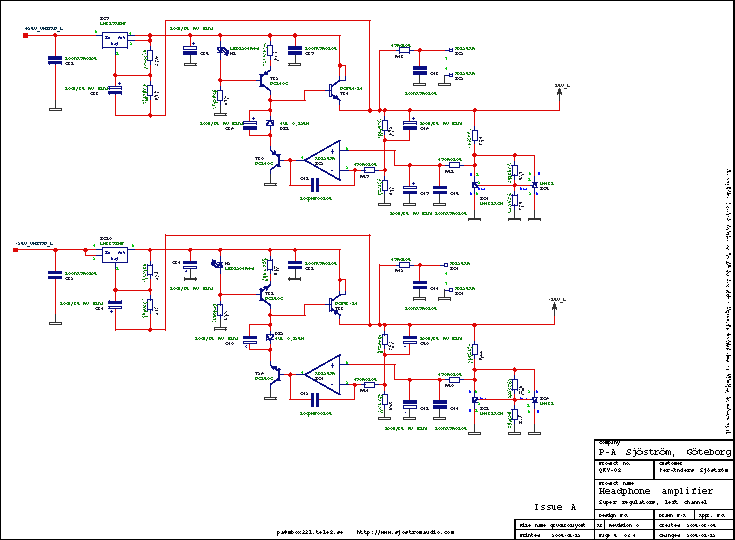
Click on the picture to get a larger view. The picture shows the schematics of the amp. Of course you can't use it for anything except for an overview. Please download the pdf-file instead if you want to see the details.
The regulator topology is called "super regulator" because of it's super performance. Please see my SSR01 for more info.
