Page 6 of 7
The PCB layout
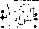
The component print
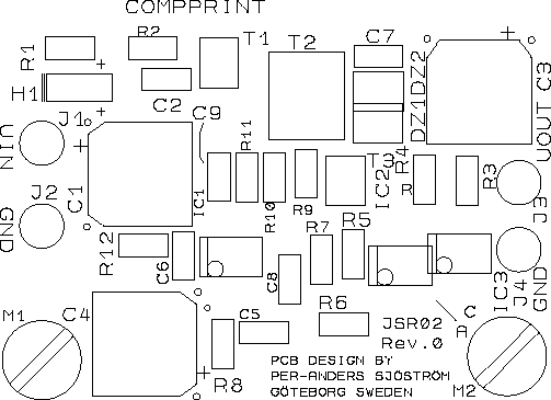
The picture shows the component print of the PCB. Of course you can't use it for anything except for an overview. Please download the pdf-file instead if you want to see the details.
The printed circuit board will be made of 50 um thick copper and has a groundplane on the solder side.
The component side
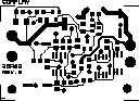
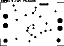
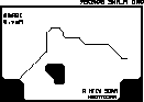
The pictures show from the left: the component side, the solder side, the groundplane mask (black areas are not groundplane) and last the thermo pads of the PCB. Please download the pdf-file instead if you want to see the details.
Most of the traces are on the component side.
